- 您现在的位置:买卖IC网 > PDF目录79850 > LT3757MPMSE#PBF (LINEAR TECHNOLOGY CORP) SWITCHING REGULATOR, 1000 kHz SWITCHING FREQ-MAX, PDSO10 PDF资料下载
参数资料
| 型号: | LT3757MPMSE#PBF |
| 厂商: | LINEAR TECHNOLOGY CORP |
| 元件分类: | 稳压器 |
| 英文描述: | SWITCHING REGULATOR, 1000 kHz SWITCHING FREQ-MAX, PDSO10 |
| 封装: | 3 X 3 MM, LEAD FREE, PLASTIC, MSOP-10 |
| 文件页数: | 6/36页 |
| 文件大小: | 436K |
| 代理商: | LT3757MPMSE#PBF |
第1页第2页第3页第4页第5页当前第6页第7页第8页第9页第10页第11页第12页第13页第14页第15页第16页第17页第18页第19页第20页第21页第22页第23页第24页第25页第26页第27页第28页第29页第30页第31页第32页第33页第34页第35页第36页
LT3757
14
3757fc
applicaTions inForMaTion
Due to the current limit function of the SENSE pin, RSENSE
shouldbeselectedtoguaranteethatthepeakcurrentsense
voltageVSENSE(PEAK)duringsteadystatenormaloperation
is lower than the SENSE current limit threshold (see the
Electrical Characteristics table). Given a 20% margin,
VSENSE(PEAK) is set to be 80mV. Then, the maximum
switch ripple current percentage can be calculated using
the following equation:
χ =
VSENSE
80mV
0.5 VSENSE
c is used in subsequent design examples to calculate in-
ductor value. VSENSE is the ripple voltage across RSENSE.
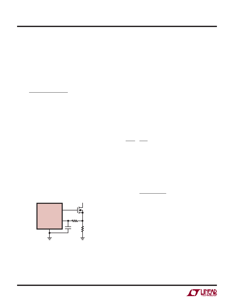
TheLT3757switchingcontrollerincorporates100nstiming
interval to blank the ringing on the current sense signal
immediately after M1 is turned on. This ringing is caused
by the parasitic inductance and capacitance of the PCB
trace, the sense resistor, the diode, and the MOSFET. The
100ns timing interval is adequate for most of the LT3757
applications. In the applications that have very large and
long ringing on the current sense signal, a small RC filter
can be added to filter out the excess ringing. Figure 5
shows the RC filter on SENSE pin. It is usually sufficient
to choose 22Ω for RFLT and 2.2nF to 10nF for CFLT.
Keep RFLT’s resistance low. Remember that there is 65A
(typical) flowing out of the SENSE pin. Adding RFLT will
affect the SENSE current limit threshold:
VSENSE_ILIM = 108mV – 65A RFLT
APPLICATION CIRCUITS
The LT3757 can be configured as different topologies. The
first topology to be analyzed will be the boost converter,
followed by the flyback, SEPIC and inverting converters.
Boost Converter: Switch Duty Cycle and Frequency
The LT3757 can be configured as a boost converter for
the applications where the converter output voltage is
higher than the input voltage. Remember that boost con-
verters are not short-circuit protected. Under a shorted
output condition, the inductor current is limited only by
the input supply capability. For applications requiring a
step-up converter that is short-circuit protected, please
refer to the Applications Information section covering
SEPIC converters.
The conversion ratio as a function of duty cycle is
VOUT
VIN
=
1
D
in continuous conduction mode (CCM).
For a boost converter operating in CCM, the duty cycle
of the main switch can be calculated based on the output
voltage (VOUT) and the input voltage (VIN). The maximum
duty cycle (DMAX) occurs when the converter has the
minimum input voltage:
DMAX =
VOUT VIN(MIN)
VOUT
Discontinuous conduction mode (DCM) provides higher
conversionratiosatagivenfrequencyatthecostofreduced
efficiencies and higher switching currents.
Figure 5. The RC Filter on SENSE Pin
CFLT
3757 F05
LT3757
RFLT
RSENSE
M1
SENSE
GATE
GND
相关PDF资料 |
PDF描述 |
|---|---|
| LM4040ESD-250GT3 | 1-OUTPUT TWO TERM VOLTAGE REFERENCE, 2.5 V, PDSO5 |
| LM4040DSD-330GT3 | 1-OUTPUT TWO TERM VOLTAGE REFERENCE, 3.3 V, PDSO5 |
| LM4040BIZ-5.0 | 1-OUTPUT TWO TERM VOLTAGE REFERENCE, 5 V, PBCY3 |
| LK5660-7EPD4TB1 | 2-OUTPUT 150 W AC-DC PWR FACTOR CORR MODULE |
| LT1374IR-5#TR | 8.5 A SWITCHING REGULATOR, 560 kHz SWITCHING FREQ-MAX, PSSO7 |
相关代理商/技术参数 |
参数描述 |
|---|---|
| LT3757MPMSE-TRPBF | 制造商:LINER 制造商全称:Linear Technology 功能描述:Boost, Flyback, SEPIC and Inverting Controller |
| LT3758 | 制造商:LINER 制造商全称:Linear Technology 功能描述:High Input Voltage, Boost, Flyback, SEPIC and Inverting Controller |
| LT3758A | 制造商:LINER 制造商全称:Linear Technology 功能描述:60V Low IQ Inverting DC/DC Controller Wide Operating VIN Range: 3.5V to 60V |
| LT3758AEDD#PBF | 制造商:Linear Technology 功能描述:IC REG CTRLR BST FLYBK INV 10DFN |
| LT3758AEDD#TRPBF | 制造商:Linear Technology 功能描述:IC REG CTRLR BST FLYBK INV 10DFN 制造商:Linear Technology 功能描述:SP-SWREG/Controller, High Input Voltage, Boost, Flyback, SEPIC and Inverting Con |
发布紧急采购,3分钟左右您将得到回复。