- 您现在的位置:买卖IC网 > PDF目录79850 > LT3757MPMSE#PBF (LINEAR TECHNOLOGY CORP) SWITCHING REGULATOR, 1000 kHz SWITCHING FREQ-MAX, PDSO10 PDF资料下载
参数资料
| 型号: | LT3757MPMSE#PBF |
| 厂商: | LINEAR TECHNOLOGY CORP |
| 元件分类: | 稳压器 |
| 英文描述: | SWITCHING REGULATOR, 1000 kHz SWITCHING FREQ-MAX, PDSO10 |
| 封装: | 3 X 3 MM, LEAD FREE, PLASTIC, MSOP-10 |
| 文件页数: | 3/36页 |
| 文件大小: | 436K |
| 代理商: | LT3757MPMSE#PBF |
第1页第2页当前第3页第4页第5页第6页第7页第8页第9页第10页第11页第12页第13页第14页第15页第16页第17页第18页第19页第20页第21页第22页第23页第24页第25页第26页第27页第28页第29页第30页第31页第32页第33页第34页第35页第36页
LT3757
11
3757fc
applicaTions inForMaTion
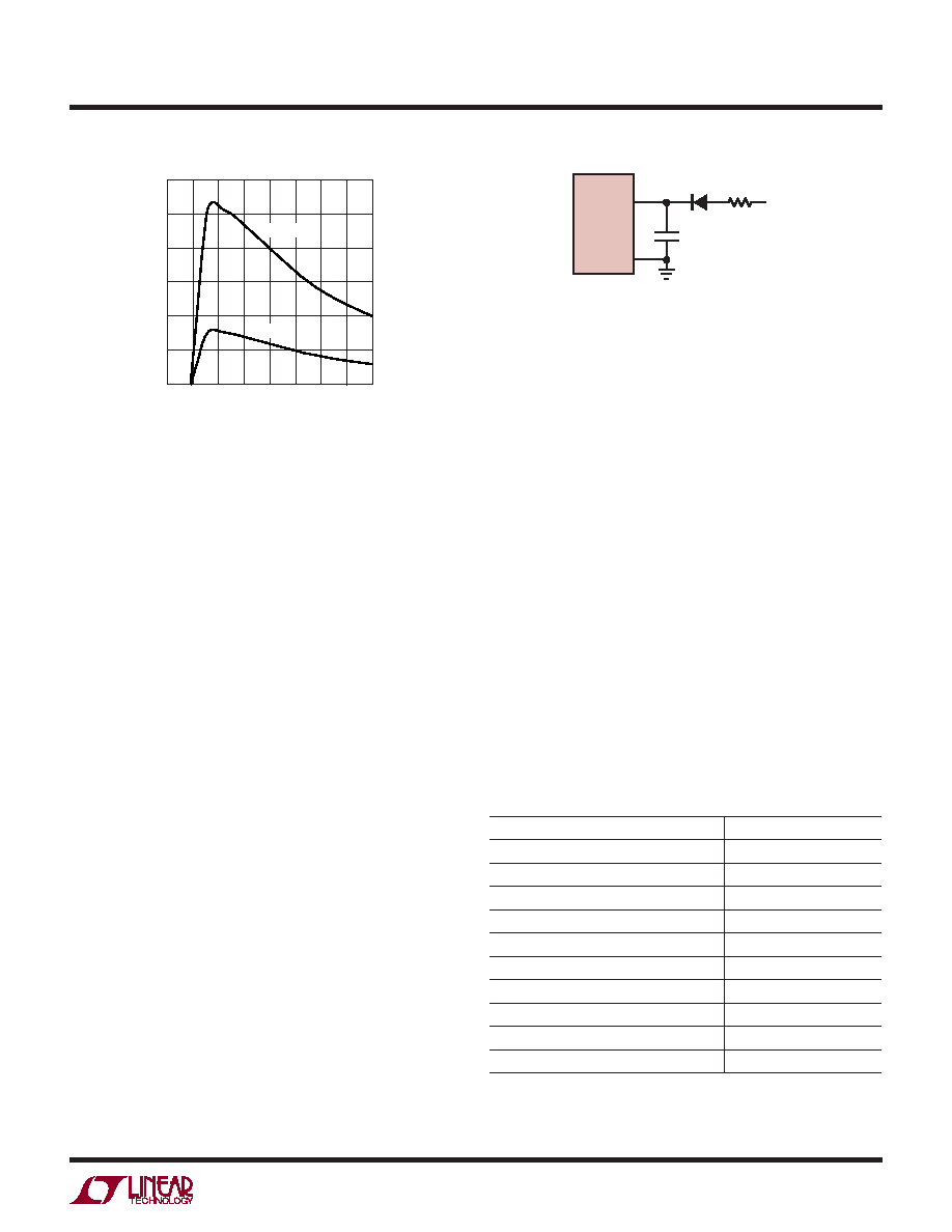
Figure 2. Recommended Maximum QG vs VIN at Different
Frequencies to Ensure INTVCC Higher Than 4.5V
An effective approach to reduce the power consumption
of the internal LDO for gate drive is to tie the INTVCC pin
to an external voltage source high enough to turn off the
internal LDO regulator.
If the input voltage VIN does not exceed the absolute
maximum rating of both the power MOSFET gate-source
voltage(VGS)andtheINTVCCovervoltagelockoutthreshold
voltage (17.5V), the INTVCC pin can be shorted directly
to the VIN pin. In this condition, the internal LDO will be
turned off and the gate driver will be powered directly
from the input voltage, VIN. With the INTVCC pin shorted to
VIN, however, a small current (around 16A) will load the
INTVCC in shutdown mode. For applications that require
the lowest shutdown mode input supply current, do not
connect the INTVCC pin to VIN.
In SEPIC or flyback applications, the INTVCC pin can be
connected to the output voltage VOUT through a blocking
diode, as shown in Figure 3, if VOUT meets the following
conditions:
1. VOUT < VIN (pin voltage)
2. 7.2 < VOUT < 17.5V
3. VOUT < maximum VGS rating of power MOSFET
A resistor RVCC can be connected, as shown in Figure 3, to
limit the inrush current from VOUT. Regardless of whether
Figure 3. Connecting INTVCC to VOUT
CVCC
4.7F
VOUT
3757 F03
INTVCC
GND
LT3757
RVCC
DVCC
VIN (V)
0
Q
G(nC)
200
250
150
100
10
20
5
15
30
40
25
35
50
0
300
3757 F02
300kHz
1MHz
or not the INTVCC pin is connected to an external voltage
source, it is always necessary to have the driver circuitry
bypassed with a 4.7F low ESR ceramic capacitor to
ground immediately adjacent to the INTVCC and GND pins.
Operating Frequency and Synchronization
The choice of operating frequency may be determined
by on-chip power dissipation, otherwise it is a trade-off
between efficiency and component size. Low frequency
operation improves efficiency by reducing gate drive cur-
rent and MOSFET and diode switching losses. However,
lower frequency operation requires a physically larger
inductor. Switching frequency also has implications for
loopcompensation.TheLT3757usesaconstant-frequency
architecture that can be programmed over a 100kHz to
1000kHz range with a single external resistor from the
RT pin to ground, as shown in Figure 1. The RT pin must
have an external resistor to GND for proper operation of
the LT3757. A table for selecting the value of RT for a given
operating frequency is shown in Table 1.
Table 1. Timing Resistor (RT) Value
OSCILLATOR FREQUENCY (kHz)
RT (kΩ)
100
140
200
63.4
300
41.2
400
30.9
500
24.3
600
19.6
700
16.5
800
14
900
12.1
1000
10.5
相关PDF资料 |
PDF描述 |
|---|---|
| LM4040ESD-250GT3 | 1-OUTPUT TWO TERM VOLTAGE REFERENCE, 2.5 V, PDSO5 |
| LM4040DSD-330GT3 | 1-OUTPUT TWO TERM VOLTAGE REFERENCE, 3.3 V, PDSO5 |
| LM4040BIZ-5.0 | 1-OUTPUT TWO TERM VOLTAGE REFERENCE, 5 V, PBCY3 |
| LK5660-7EPD4TB1 | 2-OUTPUT 150 W AC-DC PWR FACTOR CORR MODULE |
| LT1374IR-5#TR | 8.5 A SWITCHING REGULATOR, 560 kHz SWITCHING FREQ-MAX, PSSO7 |
相关代理商/技术参数 |
参数描述 |
|---|---|
| LT3757MPMSE-TRPBF | 制造商:LINER 制造商全称:Linear Technology 功能描述:Boost, Flyback, SEPIC and Inverting Controller |
| LT3758 | 制造商:LINER 制造商全称:Linear Technology 功能描述:High Input Voltage, Boost, Flyback, SEPIC and Inverting Controller |
| LT3758A | 制造商:LINER 制造商全称:Linear Technology 功能描述:60V Low IQ Inverting DC/DC Controller Wide Operating VIN Range: 3.5V to 60V |
| LT3758AEDD#PBF | 制造商:Linear Technology 功能描述:IC REG CTRLR BST FLYBK INV 10DFN |
| LT3758AEDD#TRPBF | 制造商:Linear Technology 功能描述:IC REG CTRLR BST FLYBK INV 10DFN 制造商:Linear Technology 功能描述:SP-SWREG/Controller, High Input Voltage, Boost, Flyback, SEPIC and Inverting Con |
发布紧急采购,3分钟左右您将得到回复。