- 您现在的位置:买卖IC网 > PDF目录39415 > LTC2256IUJ-14#PBF (LINEAR TECHNOLOGY CORP) 1-CH 14-BIT PROPRIETARY METHOD ADC, PARALLEL ACCESS, PQCC40 PDF资料下载
参数资料
| 型号: | LTC2256IUJ-14#PBF |
| 厂商: | LINEAR TECHNOLOGY CORP |
| 元件分类: | ADC |
| 英文描述: | 1-CH 14-BIT PROPRIETARY METHOD ADC, PARALLEL ACCESS, PQCC40 |
| 封装: | 6 X 6 MM, LEAD FREE, PLASTIC, QFN-40 |
| 文件页数: | 15/32页 |
| 文件大小: | 1546K |
| 代理商: | LTC2256IUJ-14#PBF |
第1页第2页第3页第4页第5页第6页第7页第8页第9页第10页第11页第12页第13页第14页当前第15页第16页第17页第18页第19页第20页第21页第22页第23页第24页第25页第26页第27页第28页第29页第30页第31页第32页
LTC2258-14
LTC2257-14/LTC2256-14
22
225814fa
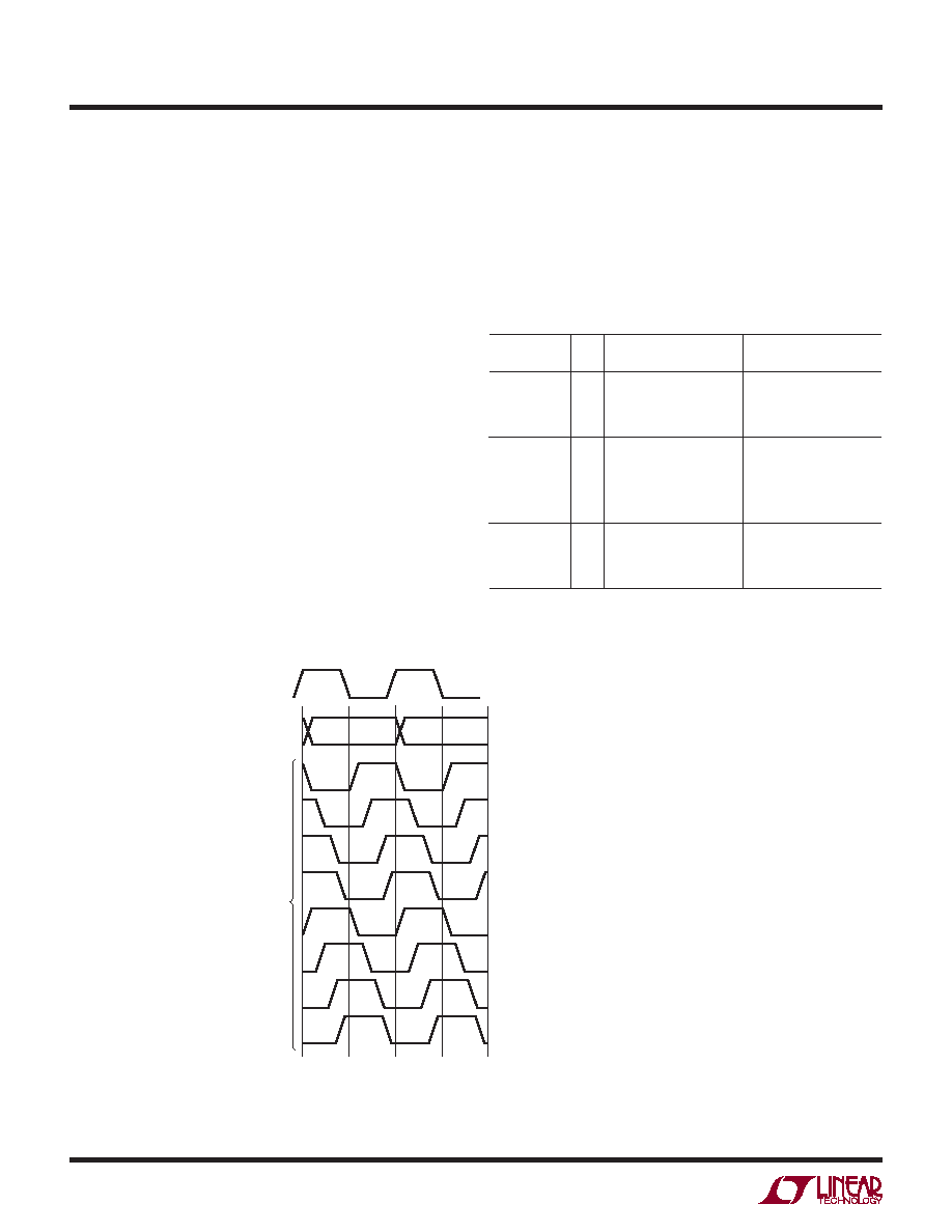
Phase Shifting the Output Clock
In full-rate CMOS mode the data output bits normally
change at the same time as the falling edge of CLKOUT+,
so the rising edge of CLKOUT+ can be used to latch the
output data. In double data rate CMOS and LVDS modes
the data output bits normally change at the same time as
the falling and rising edges of CLKOUT+. To allow adequate
setup-and-hold time when latching the data, the CLKOUT+
signal may need to be phase shifted relative to the data
output bits. Most FPGAs have this feature; this is generally
the best place to adjust the timing.
The LTC2258-14/LTC2257-14/LTC2256-14 can also phase
shift the CLKOUT+/CLKOUT– signals by serially program-
ming mode control register A2. The output clock can be
shifted by 0°, 45°, 90° or 135°. To use the phase shifting
feature the clock duty cycle stabilizer must be turned
on. Another control register bit can invert the polarity of
CLKOUT+ and CLKOUT–, independently of the phase shift.
The combination of these two features enables phase
shifts of 45° up to 315° (Figure 14).
DATA FORMAT
Table 1 shows the relationship between the analog input
voltage, the digital data output bits and the overow bit.
By default the output data format is offset binary. The 2’s
complement format can be selected by serially program-
ming mode control register A4.
Table 1. Output Codes vs Input Voltage
AIN+ – AIN–
(2V Range)
OF
D13-D0
(OFFSET BINARY)
D13-D0
(2’s COMPLEMENT)
>1.000000V
+0.999878V
+0.999756V
1
0
11 1111 1111 1111
11 1111 1111 1110
01 1111 1111 1111
01 1111 1111 1110
+0.000122V
+0.000000V
–0.000122V
–0.000244V
0
10 0000 0000 0001
10 0000 0000 0000
01 1111 1111 1111
01 1111 1111 1110
00 0000 0000 0001
00 0000 0000 0000
11 1111 1111 1111
11 1111 1111 1110
–0.999878V
–1.000000V
≤–1.000000V
0
1
00 0000 0000 0001
00 0000 0000 0000
10 0000 0000 0001
10 0000 0000 0000
APPLICATIONS INFORMATION
CLKOUT+
D0-D13, OF
PHASE
SHIFT
0°
45°
90°
135°
180°
225°
270°
315°
CLKINV
0
1
CLKPHASE1
MODE CONTROL BITS
0
1
0
1
CLKPHASE0
0
1
0
1
0
1
0
1
225814 F14
ENC+
Figure 14. Phase Shifting CLKOUT
相关PDF资料 |
PDF描述 |
|---|---|
| LTC2257CUJ-14#PBF | 1-CH 14-BIT PROPRIETARY METHOD ADC, PARALLEL ACCESS, PQCC40 |
| LTC2257IUJ-14#PBF | 1-CH 14-BIT PROPRIETARY METHOD ADC, PARALLEL ACCESS, PQCC40 |
| LTC2259CUJ-16#PBF | PROPRIETARY METHOD ADC, PQCC40 |
| LTC2259IUJ-16#PBF | PROPRIETARY METHOD ADC, PQCC40 |
| LTC2259CUJ-16#TRPBF | PROPRIETARY METHOD ADC, PQCC40 |
相关代理商/技术参数 |
参数描述 |
|---|---|
| LTC2256IUJ-14-TRPBF | 制造商:LINER 制造商全称:Linear Technology 功能描述:14-Bit, 65/40/25Msps Ultralow Power 1.8V ADCs |
| LTC2256UJ-12 | 制造商:LINER 制造商全称:Linear Technology 功能描述:12-Bit, 65/40/2 5Msps Ultralow Power 1.8V ADCs |
| LTC2256UJ-14 | 制造商:LINER 制造商全称:Linear Technology 功能描述:14-Bit, 65/40/25Msps Ultralow Power 1.8V ADCs |
| LTC2257-12 | 制造商:LINER 制造商全称:Linear Technology 功能描述:12-Bit, 65/40/2 5Msps Ultralow Power 1.8V ADCs |
| LTC2257-14 | 制造商:LINER 制造商全称:Linear Technology 功能描述:14-Bit, 65/40/25Msps Ultralow Power 1.8V ADCs |
发布紧急采购,3分钟左右您将得到回复。