- 您现在的位置:买卖IC网 > PDF目录39415 > LTC2256IUJ-14#PBF (LINEAR TECHNOLOGY CORP) 1-CH 14-BIT PROPRIETARY METHOD ADC, PARALLEL ACCESS, PQCC40 PDF资料下载
参数资料
| 型号: | LTC2256IUJ-14#PBF |
| 厂商: | LINEAR TECHNOLOGY CORP |
| 元件分类: | ADC |
| 英文描述: | 1-CH 14-BIT PROPRIETARY METHOD ADC, PARALLEL ACCESS, PQCC40 |
| 封装: | 6 X 6 MM, LEAD FREE, PLASTIC, QFN-40 |
| 文件页数: | 18/32页 |
| 文件大小: | 1546K |
| 代理商: | LTC2256IUJ-14#PBF |
第1页第2页第3页第4页第5页第6页第7页第8页第9页第10页第11页第12页第13页第14页第15页第16页第17页当前第18页第19页第20页第21页第22页第23页第24页第25页第26页第27页第28页第29页第30页第31页第32页
25
225814fa
LTC2258-14
LTC2257-14/LTC2256-14
APPLICATIONS INFORMATION
Serial Programming Mode
To use the serial programming mode, PAR/SER should be
tied to ground. The CS, SCK, SDI and SDO pins become
a serial interface that program the A/D mode control
registers. Data is written to a register with a 16-bit serial
word. Data can also be read back from a register to verify
its contents.
Serial data transfer starts when CS is taken low. The data
on the SDI pin is latched at the rst 16 rising edges of
SCK. Any SCK rising edges after the rst 16 are ignored.
The data transfer ends when CS is taken high again.
The rst bit of the 16-bit input word is the R/W bit. The
next seven bits are the address of the register (A6:A0).
The nal eight bits are the register data (D7:D0).
If the R/W bit is low, the serial data (D7:D0) will be writ-
ten to the register set by the address bits (A6:A0). If the
R/W bit is high, data in the register set by the address bits
(A6:A0) will be read back on the SDO pin (see the timing
diagrams). During a read back command the register is
not updated and data on SDI is ignored.
The SDO pin is an open-drain output that pulls to ground
with a 200Ω impedance. If register data is read back
through SDO, an external 2k pull-up resistor is required.
If serial data is only written and read back is not needed,
then SDO can be left oating and no pull-up resistor is
needed.
Table 3 shows a map of the mode control registers.
Software Reset
If serial programming is used, the mode control registers
should be programmed as soon as possible after the power
supplies turn on and are stable. The rst serial command
must be a software reset which will reset all register data
bits to logic 0. To perform a software reset, bit D7 in the
reset register is written with a logic 1. After the reset is
complete, bit D7 is automatically set back to zero.
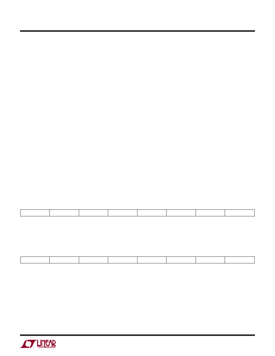
Table 3. Serial Programming Mode Register Map
REGISTER A0: RESET REGISTER (ADDRESS 00h)
D7
D6
D5
D4
D3
D2
D1
D0
RESET
XXXXXX
X
Bit 7
RESET
Software Reset Bit
0 = Not Used
1 = Software Reset. All Mode Control Registers are Reset to 00h. This Bit is Automatically Set Back to Zero After the Reset is Complete
Bits 6-0
Unused, Don’t Care Bits.
REGISTER A1: POWER-DOWN REGISTER (ADDRESS 01h)
D7
D6
D5
D4
D3
D2
D1
D0
XXXXXX
PWROFF1
PWROFF0
Bits 7-2
Unused, Don’t Care Bits.
Bits 1-0
PWROFF1:PWROFF0
Power Down Control Bits
00 = Normal Operation
01 = Nap Mode
10 = Not Used
11 = Sleep Mode
相关PDF资料 |
PDF描述 |
|---|---|
| LTC2257CUJ-14#PBF | 1-CH 14-BIT PROPRIETARY METHOD ADC, PARALLEL ACCESS, PQCC40 |
| LTC2257IUJ-14#PBF | 1-CH 14-BIT PROPRIETARY METHOD ADC, PARALLEL ACCESS, PQCC40 |
| LTC2259CUJ-16#PBF | PROPRIETARY METHOD ADC, PQCC40 |
| LTC2259IUJ-16#PBF | PROPRIETARY METHOD ADC, PQCC40 |
| LTC2259CUJ-16#TRPBF | PROPRIETARY METHOD ADC, PQCC40 |
相关代理商/技术参数 |
参数描述 |
|---|---|
| LTC2256IUJ-14-TRPBF | 制造商:LINER 制造商全称:Linear Technology 功能描述:14-Bit, 65/40/25Msps Ultralow Power 1.8V ADCs |
| LTC2256UJ-12 | 制造商:LINER 制造商全称:Linear Technology 功能描述:12-Bit, 65/40/2 5Msps Ultralow Power 1.8V ADCs |
| LTC2256UJ-14 | 制造商:LINER 制造商全称:Linear Technology 功能描述:14-Bit, 65/40/25Msps Ultralow Power 1.8V ADCs |
| LTC2257-12 | 制造商:LINER 制造商全称:Linear Technology 功能描述:12-Bit, 65/40/2 5Msps Ultralow Power 1.8V ADCs |
| LTC2257-14 | 制造商:LINER 制造商全称:Linear Technology 功能描述:14-Bit, 65/40/25Msps Ultralow Power 1.8V ADCs |
发布紧急采购,3分钟左右您将得到回复。