- 您现在的位置:买卖IC网 > PDF目录39415 > LTC2256IUJ-14#PBF (LINEAR TECHNOLOGY CORP) 1-CH 14-BIT PROPRIETARY METHOD ADC, PARALLEL ACCESS, PQCC40 PDF资料下载
参数资料
| 型号: | LTC2256IUJ-14#PBF |
| 厂商: | LINEAR TECHNOLOGY CORP |
| 元件分类: | ADC |
| 英文描述: | 1-CH 14-BIT PROPRIETARY METHOD ADC, PARALLEL ACCESS, PQCC40 |
| 封装: | 6 X 6 MM, LEAD FREE, PLASTIC, QFN-40 |
| 文件页数: | 6/32页 |
| 文件大小: | 1546K |
| 代理商: | LTC2256IUJ-14#PBF |
第1页第2页第3页第4页第5页当前第6页第7页第8页第9页第10页第11页第12页第13页第14页第15页第16页第17页第18页第19页第20页第21页第22页第23页第24页第25页第26页第27页第28页第29页第30页第31页第32页
LTC2258-14
LTC2257-14/LTC2256-14
14
225814fa
PIN FUNCTIONS
PINS THAT ARE THE SAME FOR ALL DIGITAL OUTPUT
MODES
AIN+ (Pin 1): Positive Differential Analog Input.
AIN– (Pin 2): Negative Differential Analog Input.
GND (Pin 3): ADC Power Ground.
REFH (Pins 4, 5): ADC High Reference. Bypass to Pins
6, 7 with a 2.2μF ceramic capacitor and to ground with a
0.1μF ceramic capacitor.
REFL (Pins 6, 7): ADC Low Reference. Bypass to Pins
4, 5 with a 2.2μF ceramic capacitor and to ground with a
0.1μF ceramic capacitor.
PAR/SER (Pin 8): Programming Mode Selection Pin. Con-
nect to ground to enable the serial programming mode.
CS, SCK, SDI, SDO become a serial interface that control
the A/D operating modes. Connect to VDD to enable the
parallel programming mode where CS, SCK, SDI become
parallel logic inputs that control a reduced set of the A/D
operating modes. PAR/SER should be connected directly
to ground or the VDD of the part and not be driven by a
logic signal.
VDD (Pins 9, 10, 40): 1.8V Analog Power Supply. Bypass
to ground with 0.1μF ceramic capacitors. Pins 9 and 10
can share a bypass capacitor.
ENC+ (Pin 11): Encode Input. Conversion starts on the
rising edge.
ENC– (Pin 12): Encode Complement Input. Conversion
starts on the falling edge.
CS (Pin 13): In serial programming mode, (PAR/SER =
0V), CS is the serial interface chip select input. When
CS is low, SCK is enabled for shifting data on SDI into
the mode control registers. In the parallel programming
mode (PAR/SER = VDD), CS controls the clock duty cycle
stabilizer. When CS is low, the clock duty cycle stabilizer is
turned off. When CS is high, the clock duty cycle stabilizer
is turned on. CS can be driven with 1.8V to 3.3V logic.
SCK (Pin 14): In serial programming mode, (PAR/SER =
0V), SCK is the serial interface clock input. In the parallel
programming mode (PAR/SER = VDD), SCK controls the
digital output mode. When SCK is low, the full-rate CMOS
output mode is enabled. When SCK is high, the double
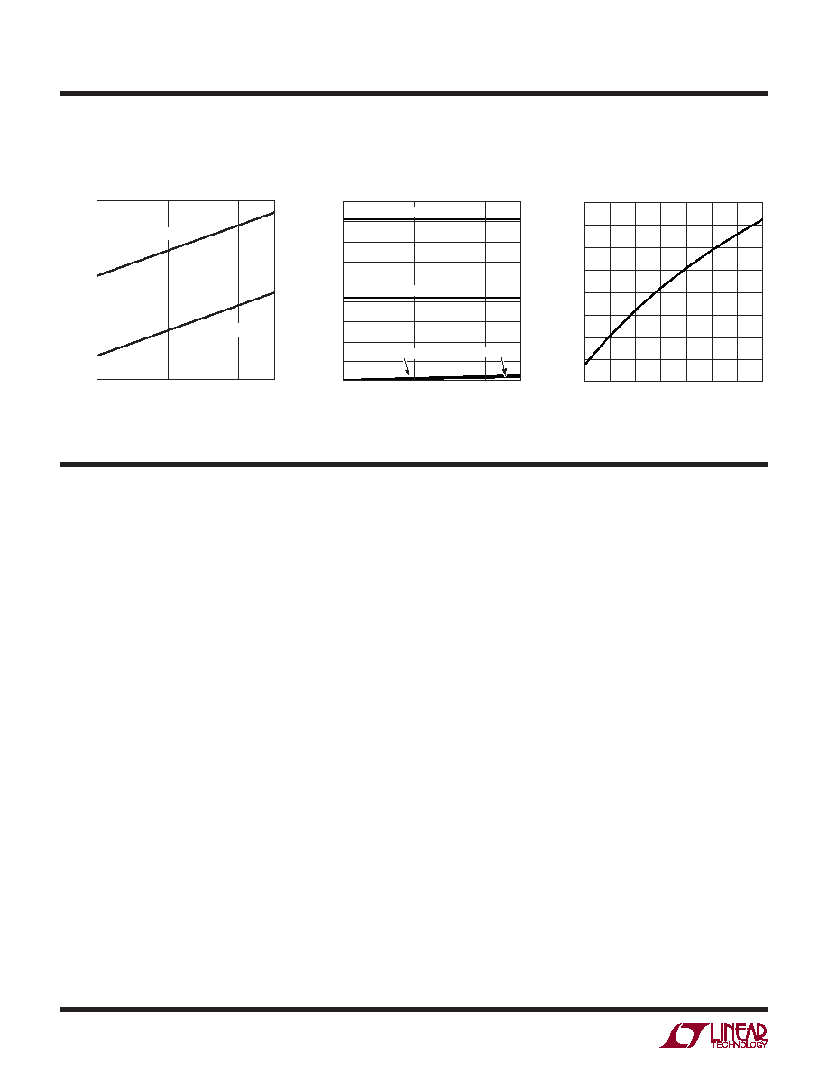
TYPICAL PERFORMANCE CHARACTERISTICS
LTC2256-14: IVDD vs Sample Rate,
5MHz Sine Wave Input, –1dB
LTC2256-14: IOVDD vs Sample Rate,
5MHz Sine Wave Input, –1dB, 5pF
on Each Data Output
LTC2256-14: SNR vs SENSE,
fIN = 5MHz, –1dB
SAMPLE RATE (Msps)
0
25
10
15
20
5
0
45
30
35
40
IOV
DD
(mA)
10
20
225814 G54
1.75mA LVDS
1.8V CMOS
1.2V CMOS
3.5mA LVDS
SAMPLE RATE (Msps)
0
15
20
25
I VDD
(mA)
10
20
225814 G53
LVDS OUTPUTS
CMOS OUTPUTS
SENSE PIN (V)
0.6
71
68
69
70
67
66
72
73
74
SNR
(dBFS)
0.7
0.8
0.9
1.1
1.2
1.3
1
225814 G55
相关PDF资料 |
PDF描述 |
|---|---|
| LTC2257CUJ-14#PBF | 1-CH 14-BIT PROPRIETARY METHOD ADC, PARALLEL ACCESS, PQCC40 |
| LTC2257IUJ-14#PBF | 1-CH 14-BIT PROPRIETARY METHOD ADC, PARALLEL ACCESS, PQCC40 |
| LTC2259CUJ-16#PBF | PROPRIETARY METHOD ADC, PQCC40 |
| LTC2259IUJ-16#PBF | PROPRIETARY METHOD ADC, PQCC40 |
| LTC2259CUJ-16#TRPBF | PROPRIETARY METHOD ADC, PQCC40 |
相关代理商/技术参数 |
参数描述 |
|---|---|
| LTC2256IUJ-14-TRPBF | 制造商:LINER 制造商全称:Linear Technology 功能描述:14-Bit, 65/40/25Msps Ultralow Power 1.8V ADCs |
| LTC2256UJ-12 | 制造商:LINER 制造商全称:Linear Technology 功能描述:12-Bit, 65/40/2 5Msps Ultralow Power 1.8V ADCs |
| LTC2256UJ-14 | 制造商:LINER 制造商全称:Linear Technology 功能描述:14-Bit, 65/40/25Msps Ultralow Power 1.8V ADCs |
| LTC2257-12 | 制造商:LINER 制造商全称:Linear Technology 功能描述:12-Bit, 65/40/2 5Msps Ultralow Power 1.8V ADCs |
| LTC2257-14 | 制造商:LINER 制造商全称:Linear Technology 功能描述:14-Bit, 65/40/25Msps Ultralow Power 1.8V ADCs |
发布紧急采购,3分钟左右您将得到回复。