- 您现在的位置:买卖IC网 > PDF目录39415 > LTC2256IUJ-14#PBF (LINEAR TECHNOLOGY CORP) 1-CH 14-BIT PROPRIETARY METHOD ADC, PARALLEL ACCESS, PQCC40 PDF资料下载
参数资料
| 型号: | LTC2256IUJ-14#PBF |
| 厂商: | LINEAR TECHNOLOGY CORP |
| 元件分类: | ADC |
| 英文描述: | 1-CH 14-BIT PROPRIETARY METHOD ADC, PARALLEL ACCESS, PQCC40 |
| 封装: | 6 X 6 MM, LEAD FREE, PLASTIC, QFN-40 |
| 文件页数: | 30/32页 |
| 文件大小: | 1546K |
| 代理商: | LTC2256IUJ-14#PBF |
第1页第2页第3页第4页第5页第6页第7页第8页第9页第10页第11页第12页第13页第14页第15页第16页第17页第18页第19页第20页第21页第22页第23页第24页第25页第26页第27页第28页第29页当前第30页第31页第32页
7
225814fa
LTC2258-14
LTC2257-14/LTC2256-14
SYMBOL
PARAMETER
CONDITIONS
MIN
TYP
MAX
UNITS
Digital Data Outputs (LVDS Mode)
tD
ENC to Data Delay
CL = 5pF (Note 8)
l
1.1
1.8
3.2
ns
tC
ENC to CLKOUT Delay
CL = 5pF (Note 8)
l
1
1.5
2.7
ns
tSKEW
DATA to CLKOUT Skew
tD – tC (Note 8)
l
0
0.3
0.6
ns
Pipeline Latency
5.5
Cycles
SPI Port Timing (Note 8)
tSCK
SCK Period
Write Mode
Readback Mode, CSDO = 20pF, RPULLUP = 2k
l
40
250
ns
tS
CS to SCK Setup Time
l
5ns
tH
SCK to CS Setup Time
l
5ns
tDS
SDI Setup Time
l
5ns
tDH
SDI Hold Time
l
5ns
tDO
SCK Falling to SDO Valid
Readback Mode, CSDO = 20pF, RPULLUP = 2k
l
125
ns
TIMING CHARACTERISTICS The l denotes the specications which apply over the full operating temperature
range, otherwise specications are at TA = 25°C. (Note 5)
Note 1: Stresses beyond those listed under Absolute Maximum Ratings
may cause permanent damage to the device. Exposure to any Absolute
Maximum Rating condition for extended periods may affect device
reliability and lifetime.
Note 2: All voltage values are with respect to GND with GND and OGND
shorted (unless otherwise noted).
Note 3: When these pin voltages are taken below GND or above VDD, they
will be clamped by internal diodes. This product can handle input currents
of greater than 100mA below GND or above VDD without latchup.
Note 4: When these pin voltages are taken below GND they will be
clamped by internal diodes. When these pin voltages are taken above VDD
they will not be clamped by internal diodes. This product can handle input
currents of greater than 100mA below GND without latchup.
Note 5: VDD = OVDD = 1.8V, fSAMPLE = 65MHz (LTC2258),
40MHz (LTC2257), or 25MHz (LTC2256), LVDS outputs with internal
termination disabled, differential ENC+/ENC– = 2VP-P sine wave, input
range = 2VP-P with differential drive, unless otherwise noted.
Note 6: Integral nonlinearity is dened as the deviation of a code from a
best t straight line to the transfer curve. The deviation is measured from
the center of the quantization band.
Note 7: Offset error is the offset voltage measured from –0.5 LSB when
the output code ickers between 00 0000 0000 0000 and 11 1111 1111
1111 in 2’s complement output mode.
Note 8: Guaranteed by design, not subject to test.
Note 9: VDD = 1.8V, fSAMPLE = 65MHz (LTC2258), 40MHz (LTC2257), or
25MHz (LTC2256), ENC+ = single-ended 1.8V square wave, ENC– = 0V,
input range = 2VP-P with differential drive, 5pF load on each digital output
unless otherwise noted.
Note 10: Recommended operating conditions.
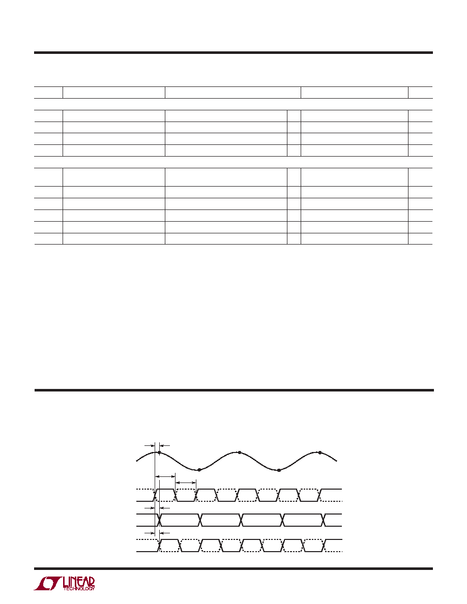
TIMING DIAGRAMS
Full-Rate CMOS Output Mode Timing
All Outputs are Single-Ended and Have CMOS Levels
tH
tD
tC
tL
N – 5
N – 4
N – 3
N – 2
N – 1
tAP
N + 1
N + 2
N + 4
N + 3
N
ANALOG
INPUT
ENC–
ENC+
CLKOUT+
CLKOUT–
D0-D13, OF
225814 TD01
相关PDF资料 |
PDF描述 |
|---|---|
| LTC2257CUJ-14#PBF | 1-CH 14-BIT PROPRIETARY METHOD ADC, PARALLEL ACCESS, PQCC40 |
| LTC2257IUJ-14#PBF | 1-CH 14-BIT PROPRIETARY METHOD ADC, PARALLEL ACCESS, PQCC40 |
| LTC2259CUJ-16#PBF | PROPRIETARY METHOD ADC, PQCC40 |
| LTC2259IUJ-16#PBF | PROPRIETARY METHOD ADC, PQCC40 |
| LTC2259CUJ-16#TRPBF | PROPRIETARY METHOD ADC, PQCC40 |
相关代理商/技术参数 |
参数描述 |
|---|---|
| LTC2256IUJ-14-TRPBF | 制造商:LINER 制造商全称:Linear Technology 功能描述:14-Bit, 65/40/25Msps Ultralow Power 1.8V ADCs |
| LTC2256UJ-12 | 制造商:LINER 制造商全称:Linear Technology 功能描述:12-Bit, 65/40/2 5Msps Ultralow Power 1.8V ADCs |
| LTC2256UJ-14 | 制造商:LINER 制造商全称:Linear Technology 功能描述:14-Bit, 65/40/25Msps Ultralow Power 1.8V ADCs |
| LTC2257-12 | 制造商:LINER 制造商全称:Linear Technology 功能描述:12-Bit, 65/40/2 5Msps Ultralow Power 1.8V ADCs |
| LTC2257-14 | 制造商:LINER 制造商全称:Linear Technology 功能描述:14-Bit, 65/40/25Msps Ultralow Power 1.8V ADCs |
发布紧急采购,3分钟左右您将得到回复。