- 您现在的位置:买卖IC网 > PDF目录1829 > LTC3425EUH#TRPBF (Linear Technology)IC REG BOOST SYNC ADJ 5A 32QFN PDF资料下载
参数资料
| 型号: | LTC3425EUH#TRPBF |
| 厂商: | Linear Technology |
| 文件页数: | 3/24页 |
| 文件大小: | 0K |
| 描述: | IC REG BOOST SYNC ADJ 5A 32QFN |
| 标准包装: | 2,500 |
| 类型: | 升压(升压) |
| 输出类型: | 可调式 |
| 输出数: | 1 |
| 输出电压: | 2.4 V ~ 5.25 V |
| 输入电压: | 0.5 V ~ 4.5 V |
| PWM 型: | 电流模式,混合 |
| 频率 - 开关: | 100kHz ~ 2MHz |
| 电流 - 输出: | 5A |
| 同步整流器: | 是 |
| 工作温度: | -40°C ~ 85°C |
| 安装类型: | 表面贴装 |
| 封装/外壳: | 32-WFQFN 裸露焊盘 |
| 包装: | 带卷 (TR) |
| 供应商设备封装: | 32-QFN 裸露焊盘(5x5) |
�� �
�
�LTC3425�
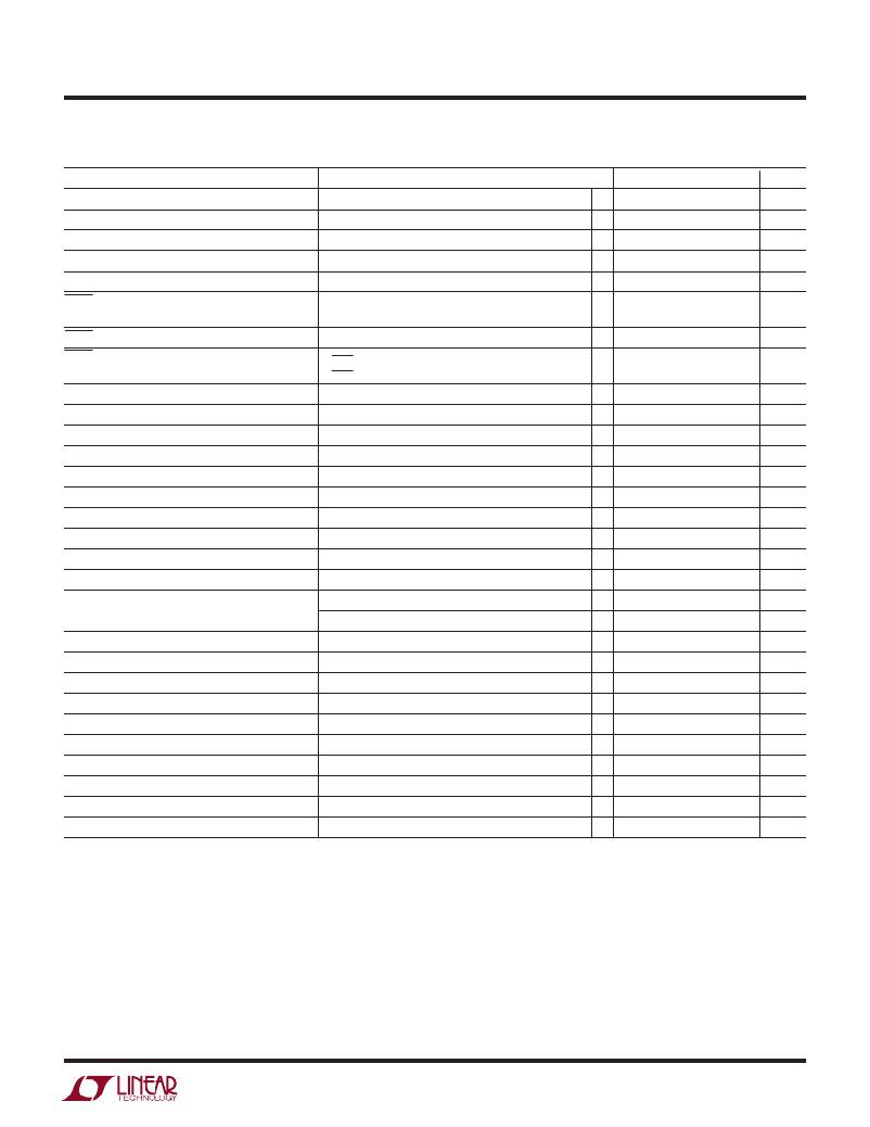
�ELECTRICAL� CHARACTERISTICS� The� q� denotes� the� specifications� which� apply� over� the� full� operating�
�temperature� range,� otherwise� specifications� are� at� T� A� =� 25� °� C.� V� IN� =� 1.2V,� V� OUT� =� 3.3V,� R� T� =� 15k,� unless� otherwise� noted.�
�PARAMETER�
�PMOS� Turn-Off� Current�
�PMOS� Reverse� Current� Limit�
�Max� Duty� Cycle�
�Min� Duty� Cycle�
�CONDITIONS�
�CCM� <� 0.4V�
�CCM� >� 1.4V�
�q�
�q�
�MIN�
�83�
�TYP�
�–80�
�0.6�
�90�
�MAX�
�97�
�0�
�UNITS�
�mA�
�A�
�%�
�%�
�Frequency� Accuracy�
�SHDN� Input� High�
�R� T� =� 15k�
�V� OUT� =� 0V� (Initial� Start-Up)�
�q�
�q�
�0.8�
�1�
�1�
�1.2�
�MHz�
�V�
�SHDN� Input� Low�
�V� OUT� >� 2.4V�
�q�
�q�
�0.65�
�0.25�
�V�
�V�
�SHDN� Input� Current�
�V� SHDN� =� 5V� or� 0V�
�V� SHDN� =� 2V�
�0.01�
�–0.50�
�1�
�μ� A�
�μ� A�
�REFEN,� CCM� Input� High�
�REFEN,� CCM� Input� Low�
�q�
�q�
�1.4�
�0.4�
�V�
�V�
�REFEN,� Input� Current�
�V� REFEN� =� 5V�
�0.01�
�1�
�μ� A�
�SYNCIN� Input� High�
�SYNCIN� Input� Low�
�(Note� 7)�
�(Note� 7)�
�q�
�q�
�2.5�
�0.5�
�V�
�V�
�SYNCIN� Input� Current�
�CCM� Input� Current�
�SYNC� Input� Pulse� Width� Range�
�V� SYNCIN� =� 5V�
�V� CCM� =� 5V�
�q�
�0.1�
�0.3�
�2�
�1�
�4�
�μ� A�
�μ� A�
�μ� s�
�SYNC� Out� High�
�SYNC� Out� Low�
�3�
�0.4�
�V�
�V�
�REFOUT�
�REFEN� >� 1.4V,� No� Load�
�I� SOURCE� <� 100� μ� A,� I� SINK� <� 10� μ� A�
�q�
�q�
�1.190�
�1.184�
�1.220�
�1.220�
�1.251�
�1.252�
�V�
�V�
�Error� Amp� Transconductance�
�50�
�μ� S�
�Error� Amp� Output� High�
�Error� Amp� Output� Low�
�I� LIM� Resistor� =� 75k�
�2.2�
�0.15�
�V�
�V�
�PGOOD� Threshold� (Falling� Edge)�
�PGOOD� Hysteresis�
�PGOOD� Low� Voltage�
�PGOOD� Leakage�
�Referenced� to� Feedback� Voltage�
�Referenced� to� Feedback� Voltage�
�I� SINK� =� 1mA� (10mA� Max)�
�V� PGOOD� =� 5.5V�
�q�
�q�
�q�
�q�
�–9.5�
�1.5�
�–11.4�
�2.5�
�0.12�
�0.01�
�–13.5�
�4�
�0.25�
�1�
�%�
�%�
�V�
�μ� A�
�SS� Current� Source�
�V� SS� =� 1V�
�2.7�
�μ� A�
�Burst� Threshold� Voltage�
�Falling� Edge�
�q�
�0.84�
�0.94�
�1.04�
�V�
�Burst� Threshold� Hysteresis�
�120�
�mV�
�Note� 1:� Absolute� Maximum� Ratings� are� those� values� beyond� which� the� life�
�of� a� device� may� be� impaired.�
�Note� 2:� Current� is� measured� into� the� V� OUTS� pin� since� the� supply� current� is�
�bootstrapped� to� the� output.� The� current� will� reflect� to� the� input� supply� by�
�V� OUT� /(V� IN� ?� Efficiency).� The� outputs� are� not� switching.�
�Note� 3:� Once� the� output� is� started,� the� IC� is� not� dependent� on� the� V� IN�
�supply.�
�Note� 4:� Total� with� all� four� FETs� in� parallel.�
�Note� 5:� The� LTC3425E� is� guaranteed� to� meet� performance� specifications�
�from� 0� °� C� to� 70� °� C.� Specifications� over� the� –40� °� C� to� 85� °� C� operating�
�temperature� range� are� assured� by� design,� characterization� and� correlation�
�with� statistical� process� controls.�
�Note� 6:� This� IC� includes� overtemperature� protection� that� is� intended� to�
�protect� the� device� during� momentary� overload� conditions.� Junction�
�temperature� will� exceed� 125� °� C� when� overtemperature� protection� is� active.�
�Continuous� operation� above� the� specified� maximum� operating� junction�
�temperature� may� impair� device� reliability.�
�Note� 7:� The� typical� logic� threshold� for� this� input� is:� V� OUT� /2�
�3425f�
�3�
�相关PDF资料 |
PDF描述 |
|---|---|
| LTC3426ES6#TRPBF | IC REG BOOST ADJ 2A TSOT23-6 |
| LTC3427EDC#TRPBF | IC REG BOOST SYNC ADJ 0.5A 6DFN |
| LTC3428EDD#TRPBF | IC REG BOOST ADJ 4A 10DFN |
| LTC3429ES6#TRM | IC REG BST SYNC ADJ .6A TSOT23-6 |
| LTC3440EDD#TRPBF | IC REG BUCK BOOST SYNC ADJ 10DFN |
相关代理商/技术参数 |
参数描述 |
|---|---|
| LTC3426 | 制造商:LINER 制造商全称:Linear Technology 功能描述:1.2MHz Step-Up DC/DC Converter in SOT-23 |
| LTC3426ES6 | 制造商:Linear Technology 功能描述:Conv DC-DC Single Step Up 1.6V to 4.3V 6-Pin TSOT-23 |
| LTC3426ES6#PBF | 制造商:Linear Technology 功能描述:Conv DC-DC Single Step Up 1.6V to 4.3V 6-Pin TSOT-23 |
| LTC3426ES6#TRM | 制造商:Linear Technology 功能描述:Conv DC-DC Single Step Up 1.6V to 4.3V 6-Pin TSOT-23 T/R |
| LTC3426ES6#TRMPBF | 功能描述:IC REG BOOST ADJ 2A TSOT23-6 RoHS:是 类别:集成电路 (IC) >> PMIC - 稳压器 - DC DC 开关稳压器 系列:- 产品培训模块:High Efficiency Current Mode Switching Regulators CMOS LDO Regulators 特色产品:BD91x Series Step-Down Regulators 标准包装:2,500 系列:- 类型:降压(降压) 输出类型:两者兼有 输出数:2 输出电压:3.3V,0.8 V ~ 2.5 V 输入电压:4.5 V ~ 5.5 V PWM 型:电流模式 频率 - 开关:1MHz 电流 - 输出:1.5A 同步整流器:是 工作温度:-40°C ~ 85°C 安装类型:表面贴装 封装/外壳:20-VFQFN 裸露焊盘 包装:带卷 (TR) 供应商设备封装:VQFN020V4040 产品目录页面:1373 (CN2011-ZH PDF) 其它名称:BD9152MUV-E2TR |
发布紧急采购,3分钟左右您将得到回复。