- 您现在的位置:买卖IC网 > PDF目录44991 > LTC3553EUD#PBF (LINEAR TECHNOLOGY CORP) 1-CHANNEL POWER SUPPLY SUPPORT CKT, PQCC20 PDF资料下载
参数资料
| 型号: | LTC3553EUD#PBF |
| 厂商: | LINEAR TECHNOLOGY CORP |
| 元件分类: | 电源管理 |
| 英文描述: | 1-CHANNEL POWER SUPPLY SUPPORT CKT, PQCC20 |
| 封装: | 3 X 3 MM, 0.75 MM HEIGHT, LEAD FREE, PLASTIC, QFN-20 |
| 文件页数: | 33/36页 |
| 文件大小: | 518K |
| 代理商: | LTC3553EUD#PBF |
第1页第2页第3页第4页第5页第6页第7页第8页第9页第10页第11页第12页第13页第14页第15页第16页第17页第18页第19页第20页第21页第22页第23页第24页第25页第26页第27页第28页第29页第30页第31页第32页当前第33页第34页第35页第36页
LTC3553
6
3553fa
Note 1: Stresses beyond those listed under Absolute Maximum Ratings
may cause permanent damage to the device. Exposure to any Absolute
Maximum Rating condition for extended periods may affect device
reliability and lifetime.
Note 2: The LTC3553E is tested under pulsed load conditions such
that TJ ≈ TA. The LTC3553E is guaranteed to meet specications from
0°C to 85°C junction temperature. Specications over the –40°C to
85°C operating junction temperature range are assured by design,
characterization and correlation with statistical process controls.
The junction temperature (TJ, in °C) is calculated from the ambient
temperature (TA, in °C) and power dissipation (PD, in Watts) according
to the formula: TJ = TA + (PD θJA), where θJA (in °C/W) is the package
thermal impedance.
Note that the maximum ambient temperature consistent with these
specications is determined by specic operating conditions in
conjunction with board layout, the rated package thermal impedance and
other environmental factors.
Note 3: This IC includes overtemperature protection that is intended
to protect the device during momentary overload conditions. Junction
temperatures will exceed 110°C when overtemperature protection is
active. Continuous operation above the specied maximum operating
junction temperature may result in device degradation or failure.
Note 4: VCC is the greater of VBUS or BAT.
Note 5: Total battery drain current represents the load a battery will see
in application due to quiescent currents drawn by the BAT pin (IBATQ)
plus any current drawn from the VOUT pin. In applications where the
buck input (BVIN pin) and LDO input (VINLDO pin) are connected to the
PowerPath output (VOUT pin), the quiescent currents on BVIN and VINLDO
must be added to IBATQ to get the actual battery drain current that will be
seen in application.
Note 6: hC/10 is expressed as a fraction of programmed full charge
current with specied PROG resistor.
Note 7: The current limit features of this part are intended to protect
the IC from short term or intermittent fault conditions. Continuous
operation above the absolute maximum specied pin current rating may
result in device degradation or failure.
Note 8: BUCK_FB High, Not Switching
Note 9: VOUT not in UVLO.
Note 10: Measured with the LDO operating in unity-gain, with its output
and feedback pins tied together.
Note 11: See the Operation section of this data sheet for detailed
explanation of the pushbutton state machine and the effects of each
state on regulator and power manager operation.
Note 12: If VBUS < VUVLO then VFWD = 0 and the forward voltage across
the ideal diode is equal to its current times RDROPOUT.
Note 13: Dropout voltage is the minimum input to output voltage
differential needed for the LDO to maintain regulation at a specied
output current. When the LDO is in dropout, its output voltage will be
equal to: VINLDO – VDROP.
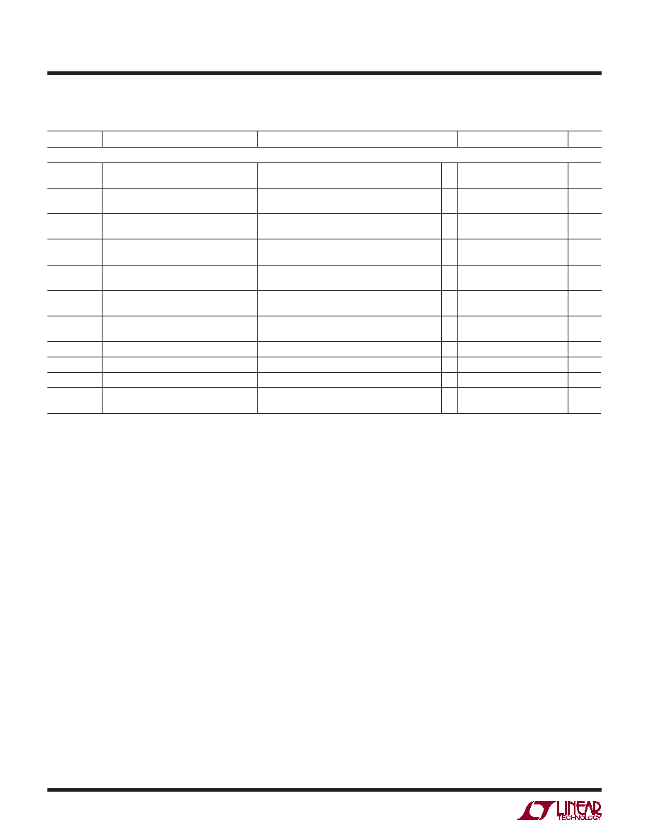
PUSHBUTTON INTERFACE ELECTRICAL CHARACTERISTICS
The
l denotes specications that apply over the full operating temperature range, otherwise specications are at TA = 25°C (Note 2).
VBAT = 3.8V, unless otherwise noted.
SYMBOL
PARAMETER
CONDITIONS
MIN
TYP
MAX
UNITS
Pushbutton Timing Parameters (Note 11)
tON_PBSTATL
Minimum ON Low Time to Cause
PBSTAT Low
ON Brought Low During Power-On (PON) or
Power-Up (PUP1, PUP2) States
50
ms
tON_PBSTATH
Delay from ON High to PBSTAT High
Power-On (PON) State, After PBSTAT Has Been
Low for at Least tPBSTAT_PW
900
μs
tON_PUP
Minimum ON Low Time to Enter
Power-Up (PUP1 or PUP2) State
Starting in the Hard Reset (HR) or Power-Off
(POFF) States
400
ms
tON_HR
Minimum ON Low Time to Hard Reset
ON Brought Low During the Power-On (PON) or
Power-Up (PUP1, PUP2) States
45
6
s
tPBSTAT_PW
PBSTAT Minimum Pulse Width
Power-On (PON) or Power-Up (PUP1, PUP2)
States
40
50
ms
tEXTPWR
Power-Up from USB Present to
Power-Up (PUP1 or PUP2) State
Starting in the Hard Reset (HR) or Power-Off
(POFF) States
100
ms
tPON_UP
BUCK_ON or LDO_ON High to Power-On
State
Starting with Both BUCK_ON and LDO_ON Low
in the Power-Off (POFF) State
900
μs
tPON_DIS_BUCK BUCK_ON Low to Buck Disabled
1
μs
tPON_DIS_LDO
LDO_ON Low to LDO Disabled
1μs
tPUP
Power-Up (PUP1 or PUP2) State Duration
5
s
tPDN
Power-Down (PDN1 or PDN2) State
Duration
1s
相关PDF资料 |
PDF描述 |
|---|---|
| LTC3554EPD#TRPB | 0.5 A BATTERY CHARGE CONTROLLER, 1295 kHz SWITCHING FREQ-MAX, PQCC20 |
| LTC3560IS6#TRPBF | 2.1 A SWITCHING REGULATOR, 2700 kHz SWITCHING FREQ-MAX, PDSO6 |
| LTC3563EDC | 1.75 A SWITCHING REGULATOR, 2700 kHz SWITCHING FREQ-MAX, PDSO6 |
| LTC3568EDD#TR | 4 A SWITCHING REGULATOR, 4000 kHz SWITCHING FREQ-MAX, PDSO10 |
| LTC3568IDD | 4 A SWITCHING REGULATOR, 4000 kHz SWITCHING FREQ-MAX, PDSO10 |
相关代理商/技术参数 |
参数描述 |
|---|---|
| LTC3554 | 制造商:LINER 制造商全称:Linear Technology 功能描述:Micropower USB Power Manager with Li-Ion Charger and Two Step-Down Regulators |
| LTC3554EPD | 制造商:LINER 制造商全称:Linear Technology 功能描述:Micropower USB Power Manager with Li-Ion Charger and Two Step-Down Regulators |
| LTC3554EPD#PBF | 功能描述:IC USB POWER MANAGER 20-UTQFN RoHS:是 类别:集成电路 (IC) >> PMIC - 电源管理 - 专用 系列:- 标准包装:1 系列:- 应用:手持/移动设备 电流 - 电源:- 电源电压:3 V ~ 5.5 V 工作温度:-40°C ~ 85°C 安装类型:表面贴装 封装/外壳:14-WFDFN 裸露焊盘 供应商设备封装:14-LLP-EP(4x4) 包装:Digi-Reel® 配用:LP3905SD-30EV-ND - BOARD EVALUATION LP3905SD-30 其它名称:LP3905SD-30DKR |
| LTC3554EPD#TRPBF | 功能描述:IC USB POWER MANAGER 20-UTQFN RoHS:是 类别:集成电路 (IC) >> PMIC - 电源管理 - 专用 系列:- 应用说明:Ultrasound Imaging Systems Application Note 产品培训模块:Lead (SnPb) Finish for COTS Obsolescence Mitigation Program 标准包装:37 系列:- 应用:医疗用超声波成像,声纳 电流 - 电源:- 电源电压:2.37 V ~ 6 V 工作温度:0°C ~ 70°C 安装类型:表面贴装 封装/外壳:56-WFQFN 裸露焊盘 供应商设备封装:56-TQFN-EP(8x8) 包装:管件 |
| LTC3554EPDPBF | 制造商:LINER 制造商全称:Linear Technology 功能描述:Micropower USB Power Manager with Li-Ion Charger and Two Step-Down Regulators |
发布紧急采购,3分钟左右您将得到回复。