- 您现在的位置:买卖IC网 > PDF目录15502 > LTC3732CG (Linear Technology)IC REG CTRLR BUCK PWM CM 36-SSOP PDF资料下载
参数资料
| 型号: | LTC3732CG |
| 厂商: | Linear Technology |
| 文件页数: | 13/28页 |
| 文件大小: | 0K |
| 描述: | IC REG CTRLR BUCK PWM CM 36-SSOP |
| 标准包装: | 37 |
| PWM 型: | 电流模式 |
| 输出数: | 1 |
| 频率 - 最大: | 750kHz |
| 占空比: | 98.5% |
| 电源电压: | 4.5 V ~ 7 V |
| 降压: | 是 |
| 升压: | 无 |
| 回扫: | 无 |
| 反相: | 无 |
| 倍增器: | 无 |
| 除法器: | 无 |
| Cuk: | 无 |
| 隔离: | 无 |
| 工作温度: | 0°C ~ 70°C |
| 封装/外壳: | 36-SSOP(0.209",5.30mm 宽) |
| 包装: | 管件 |
| 产品目录页面: | 1335 (CN2011-ZH PDF) |
第1页第2页第3页第4页第5页第6页第7页第8页第9页第10页第11页第12页当前第13页第14页第15页第16页第17页第18页第19页第20页第21页第22页第23页第24页第25页第26页第27页第28页
�� �
�
�LTC3732�
�APPLICATIO� S� I� FOR� ATIO�
�tions� having� a� highly� varying� input� voltage,� additional�
�phases� will� produce� the� best� results.�
�Accepting� larger� values� of� ?� I� L� allows� the� use� of� low�
�inductances� but� can� result� in� higher� output� voltage� ripple.�
�A� reasonable� starting� point� for� setting� ripple� current� is�
�?� I� L� =� 0.4(I� OUT� )/N,� where� N� is� the� number� of� channels� and�
�I� OUT� is� the� total� load� current.� Remember,� the� maximum�
�?� I� L� occurs� at� the� maximum� input� voltage.� The� individual�
�inductor� ripple� currents� are� constant� determined� by� the�
�inductor,� input� and� output� voltages.�
�inductor� ripple� current� and� consequent� output� voltage�
�ripple.� Do� not� allow� the� core� to� saturate!�
�Molypermalloy� (from� Magnetics,� Inc.)� is� a� very� good,� low�
�loss� core� material� for� toroids,� but� it� is� more� expensive� than�
�ferrite.� A� reasonable� compromise� from� the� same� manu-�
�facturer� is� Kool� M� μ� .� Toroids� are� very� space� efficient,�
�especially� when� you� can� use� several� layers� of� wire.� Be-�
�cause� they� lack� a� bobbin,� mounting� is� more� difficult.�
�However,� designs� for� surface� mount� are� available� which�
�do� not� increase� the� height� significantly.�
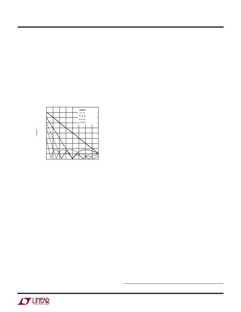
�1.0�
�0.9�
�0.8�
�0.7�
�0.6�
�0.5�
�0.4�
�0.3�
�0.2�
�0.1�
�1-PHASE�
�2-PHASE�
�3-PHASE�
�4-PHASE�
�6-PHASE�
�Power� MOSFET� and� D1,� D2,� D3� Selection�
�At� least� two� external� power� MOSFETs� must� be� selected� for�
�each� of� the� three� output� sections:� One� N-channel� MOSFET�
�for� the� top� (main)� switch� and� one� or� more� N-channel�
�MOSFET(s)� for� the� bottom� (synchronous)� switch.� The�
�number,� type� and� “on”� resistance� of� all� MOSFETs� selected�
�take� into� account� the� voltage� step-down� ratio� as� well� as� the�
�actual� position� (main� or� synchronous)� in� which� the� MOSFET�
�will� be� used.� A� much� smaller� and� much� lower� input�
�0�
�0.1�
�0.2�
�0.3� 0.4� 0.5� 0.6� 0.7�
�DUTY� FACTOR� (V� OUT� /V� IN� )�
�0.8�
�0.9�
�capacitance� MOSFET� should� be� used� for� the� top� MOSFET�
�in� applications� that� have� an� output� voltage� that� is� less� than�
�3732� F04�
�Figure� 4.� Normalized� Peak� Output� Current�
�vs� Duty� Factor� [I� RMS� =� 0.3(I� O(P-P)� ]�
�Inductor� Core� Selection�
�Once� the� value� for� L1� to� L3� is� determined,� the� type� of�
�inductor� must� be� selected.� High� efficiency� converters�
�generally� cannot� afford� the� core� loss� found� in� low� cost�
�powdered� iron� cores,� forcing� the� use� of� ferrite,�
�molypermalloy� or� Kool� M� μ� ?� cores.� Actual� core� loss� is�
�independent� of� core� size� for� a� fixed� inductor� value,� but� it�
�is� very� dependent� on� inductance� selected.� As� inductance�
�increases,� core� losses� go� down.� Unfortunately,� increased�
�inductance� requires� more� turns� of� wire� and� therefore�
�copper� losses� will� increase.�
�Ferrite� designs� have� very� low� core� loss� and� are� preferred�
�at� high� switching� frequencies,� so� design� goals� can�
�concentrate� on� copper� loss� and� preventing� saturation.�
�Ferrite� core� material� saturates� “hard,”� which� means� that�
�inductance� collapses� abruptly� when� the� peak� design�
�1/3� of� the� input� voltage.� In� applications� where� V� IN� >>� V� OUT� ,�
�the� top� MOSFETs’� “on”� resistance� is� normally� less� impor-�
�tant� for� overall� efficiency� than� its� input� capacitance� at�
�operating� frequencies� above� 300kHz.� MOSFET� manufac-�
�turers� have� designed� special� purpose� devices� that� provide�
�reasonably� low� “on”� resistance� with� significantly� reduced�
�input� capacitance� for� the� main� switch� application� in� switch-�
�ing� regulators.�
�The� peak-to-peak� MOSFET� gate� drive� levels� are� set� by� the�
�voltage,� V� CC� ,� requiring� the� use� of� logic-level� threshold�
�MOSFETs� in� most� applications.� Pay� close� attention� to� the�
�BV� DSS� specification� for� the� MOSFETs� as� well;� many� of� the�
�logic-level� MOSFETs� are� limited� to� 30V� or� less.�
�Selection� criteria� for� the� power� MOSFETs� include� the� “on”�
�resistance� R� DS(ON)� ,� input� capacitance,� input� voltage� and�
�maximum� output� current.�
�MOSFET� input� capacitance� is� a� combination� of� several�
�components� but� can� be� taken� from� the� typical� “gate�
�charge”� curve� included� on� most� data� sheets� (Figure� 5).�
�current� is� exceeded.� This� results� in� an� abrupt� increase� in�
�Kool� M� μ� is� a� registered� trademark� of� Magnetics,� Inc.�
�3732f�
�13�
�相关PDF资料 |
PDF描述 |
|---|---|
| HBC26DRTF | CONN EDGECARD 52POS DIP .100 SLD |
| LTC1735CF#PBF | IC REG CTRLR BUCK PWM CM 20TSSOP |
| GBC60DRXS | CONN EDGECARD 120PS DIP .100 SLD |
| GSC22DRTN | CONN EDGECARD 44POS DIP .100 SLD |
| GMC22DRTN | CONN EDGECARD 44POS DIP .100 SLD |
相关代理商/技术参数 |
参数描述 |
|---|---|
| LTC3732CG#PBF | 功能描述:IC REG CTRLR BUCK PWM CM 36-SSOP RoHS:是 类别:集成电路 (IC) >> PMIC - 稳压器 - DC DC 切换控制器 系列:- 标准包装:2,000 系列:- PWM 型:电流模式 输出数:1 频率 - 最大:1MHz 占空比:50% 电源电压:9 V ~ 10 V 降压:无 升压:是 回扫:是 反相:无 倍增器:无 除法器:无 Cuk:无 隔离:无 工作温度:-40°C ~ 85°C 封装/外壳:8-TSSOP(0.173",4.40mm 宽) 包装:带卷 (TR) |
| LTC3732CG#TR | 功能描述:IC REG CTRLR BUCK PWM CM 36-SSOP RoHS:否 类别:集成电路 (IC) >> PMIC - 稳压器 - DC DC 切换控制器 系列:- 标准包装:4,500 系列:PowerWise® PWM 型:控制器 输出数:1 频率 - 最大:1MHz 占空比:95% 电源电压:2.8 V ~ 5.5 V 降压:是 升压:无 回扫:无 反相:无 倍增器:无 除法器:无 Cuk:无 隔离:无 工作温度:-40°C ~ 125°C 封装/外壳:6-WDFN 裸露焊盘 包装:带卷 (TR) 配用:LM1771EVAL-ND - BOARD EVALUATION LM1771 其它名称:LM1771SSDX |
| LTC3732CG#TRPBF | 功能描述:IC REG CTRLR BUCK PWM CM 36-SSOP RoHS:否 类别:集成电路 (IC) >> PMIC - 稳压器 - DC DC 切换控制器 系列:- 标准包装:4,500 系列:PowerWise® PWM 型:控制器 输出数:1 频率 - 最大:1MHz 占空比:95% 电源电压:2.8 V ~ 5.5 V 降压:是 升压:无 回扫:无 反相:无 倍增器:无 除法器:无 Cuk:无 隔离:无 工作温度:-40°C ~ 125°C 封装/外壳:6-WDFN 裸露焊盘 包装:带卷 (TR) 配用:LM1771EVAL-ND - BOARD EVALUATION LM1771 其它名称:LM1771SSDX |
| LTC3732CUHF | 功能描述:IC REG CTRLR BUCK PWM CM 38-QFN RoHS:否 类别:集成电路 (IC) >> PMIC - 稳压器 - DC DC 切换控制器 系列:- 标准包装:4,500 系列:PowerWise® PWM 型:控制器 输出数:1 频率 - 最大:1MHz 占空比:95% 电源电压:2.8 V ~ 5.5 V 降压:是 升压:无 回扫:无 反相:无 倍增器:无 除法器:无 Cuk:无 隔离:无 工作温度:-40°C ~ 125°C 封装/外壳:6-WDFN 裸露焊盘 包装:带卷 (TR) 配用:LM1771EVAL-ND - BOARD EVALUATION LM1771 其它名称:LM1771SSDX |
| LTC3732CUHF#PBF | 功能描述:IC REG CTRLR BUCK PWM CM 38-QFN RoHS:是 类别:集成电路 (IC) >> PMIC - 稳压器 - DC DC 切换控制器 系列:- 标准包装:4,500 系列:PowerWise® PWM 型:控制器 输出数:1 频率 - 最大:1MHz 占空比:95% 电源电压:2.8 V ~ 5.5 V 降压:是 升压:无 回扫:无 反相:无 倍增器:无 除法器:无 Cuk:无 隔离:无 工作温度:-40°C ~ 125°C 封装/外壳:6-WDFN 裸露焊盘 包装:带卷 (TR) 配用:LM1771EVAL-ND - BOARD EVALUATION LM1771 其它名称:LM1771SSDX |
发布紧急采购,3分钟左右您将得到回复。