- 您现在的位置:买卖IC网 > PDF目录15502 > LTC3732CG (Linear Technology)IC REG CTRLR BUCK PWM CM 36-SSOP PDF资料下载
参数资料
| 型号: | LTC3732CG |
| 厂商: | Linear Technology |
| 文件页数: | 15/28页 |
| 文件大小: | 0K |
| 描述: | IC REG CTRLR BUCK PWM CM 36-SSOP |
| 标准包装: | 37 |
| PWM 型: | 电流模式 |
| 输出数: | 1 |
| 频率 - 最大: | 750kHz |
| 占空比: | 98.5% |
| 电源电压: | 4.5 V ~ 7 V |
| 降压: | 是 |
| 升压: | 无 |
| 回扫: | 无 |
| 反相: | 无 |
| 倍增器: | 无 |
| 除法器: | 无 |
| Cuk: | 无 |
| 隔离: | 无 |
| 工作温度: | 0°C ~ 70°C |
| 封装/外壳: | 36-SSOP(0.209",5.30mm 宽) |
| 包装: | 管件 |
| 产品目录页面: | 1335 (CN2011-ZH PDF) |
第1页第2页第3页第4页第5页第6页第7页第8页第9页第10页第11页第12页第13页第14页当前第15页第16页第17页第18页第19页第20页第21页第22页第23页第24页第25页第26页第27页第28页
�� �
�
�LTC3732�
�APPLICATIO� S� I� FOR� ATIO�
�A� 2A� to� 8A� Schottky� is� generally� a� good� compromise� for�
�both� regions� of� operation� due� to� the� relatively� small�
�average� current.� Larger� diodes� result� in� additional� transi-�
�tion� loss� due� to� their� larger� junction� capacitance.�
�C� IN� and� C� OUT� Selection�
�In� continuous� mode,� the� source� current� of� each� top�
�N-channel� MOSFET� is� a� square� wave� of� duty� cycle� V� OUT� /V� IN� .�
�A� low� ESR� input� capacitor� sized� for� the� maximum� RMS�
�current� must� be� used.� The� details� of� a� close� form� equation�
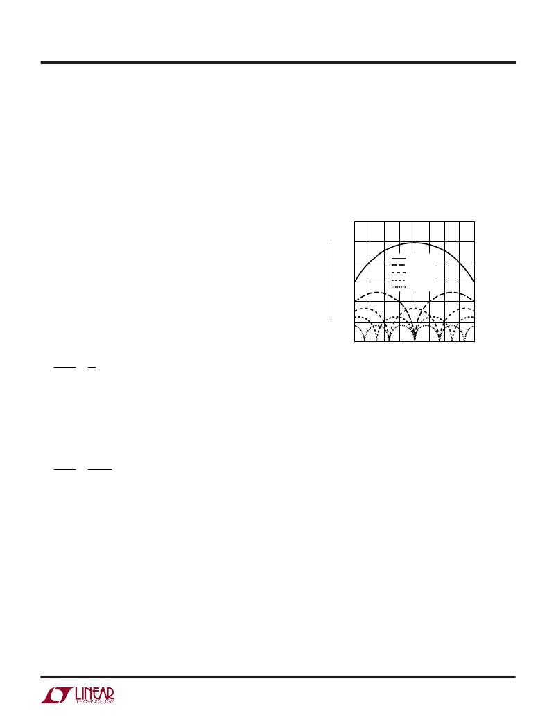
�can� be� found� in� Application� Note� 77.� Figure� 6� shows� the�
�input� capacitor� ripple� current� for� different� phase� configu-�
�therefore� a� 3-stage� implementation� results� in� 90%� less�
�power� loss� when� compared� to� a� single� phase� design.�
�Battery/input� protection� fuse� resistance� (if� used),� PC�
�board� trace� and� connector� resistance� losses� are� also�
�reduced� by� the� reduction� of� the� input� ripple� current� in� a�
�PolyPhase� system.� The� required� amount� of� input� capaci-�
�tance� is� further� reduced� by� the� factor,� N,� due� to� the�
�effective� increase� in� the� frequency� of� the� current� pulses.�
�0.6�
�0.5�
�rations� with� the� output� voltage� fixed� and� input� voltage�
�varied.� The� input� ripple� current� is� normalized� against� the�
�DC� output� current.� The� graph� can� be� used� in� place� of�
�tedious� calculations.� The� minimum� input� ripple� current�
�can� be� achieved� when� the� product� of� phase� number� and�
�output� voltage,� N(V� OUT� ),� is� approximately� equal� to� the�
�0.4�
�0.3�
�0.2�
�0.1�
�1-PHASE�
�2-PHASE�
�3-PHASE�
�4-PHASE�
�6-PHASE�
�input� voltage� V� IN� or:�
�0�
�0.1�
�0.2�
�0.3� 0.4� 0.5� 0.6� 0.7�
�0.8�
�0.9�
�V� OUT�
�V� IN�
�=�
�k�
�N�
�where� k� =� 1� ,� 2� ,� ...,� N� –� 1�
�DUTY� FACTOR� (V� OUT� /V� IN� )�
�3732� F06�
�Figure� 6.� Normalized� Input� RMS� Ripple� Current�
�So� the� phase� number� can� be� chosen� to� minimize� the� input�
�capacitor� size� for� the� given� input� and� output� voltages.�
�In� the� graph� of� Figure� 4,� the� local� maximum� input� RMS�
�capacitor� currents� are� reached� when:�
�vs� Duty� Factor� for� One� to� Six� Output� Stages�
�Ceramic� capacitors� are� becoming� very� popular� for� small�
�designs� but� several� cautions� should� be� observed.� “X7R”,�
�“X5R”� and� “Y5V”� are� examples� of� a� few� of� the� ceramic�
�materials� used� as� the� dielectric� layer,� and� these� different�
�V� OUT�
�V� IN�
�=�
�2� k� –� 1�
�N�
�where� k� =� 1� ,� 2� ,� ...,� N�
�dielectrics� have� very� different� effect� on� the� capacitance�
�value� due� to� the� voltage� and� temperature� conditions�
�These� worst-case� conditions� are� commonly� used� for� de-�
�sign� because� even� significant� deviations� do� not� offer� much�
�relief.� Note� that� capacitor� manufacturer’s� ripple� current�
�ratings� are� often� based� on� only� 2000� hours� of� life.� This�
�makes� it� advisable� to� further� derate� the� capacitor� or� to�
�choose� a� capacitor� rated� at� a� higher� temperature� than� re-�
�quired.� Several� capacitors� may� also� be� paralleled� to� meet�
�size� or� height� requirements� in� the� design.� Always� consult�
�the� capacitor� manufacturer� if� there� is� any� question.�
�The� Figure� 6� graph� shows� that� the� peak� RMS� input� current�
�is� reduced� linearly,� inversely� proportional� to� the� number� N�
�of� stages� used.� It� is� important� to� note� that� the� efficiency�
�loss� is� proportional� to� the� input� RMS� current� squared� and�
�applied.� Physically,� if� the� capacitance� value� changes� due�
�to� applied� voltage� change,� there� is� a� concommitant� piezo�
�effect� which� results� in� radiating� sound!� A� load� that� draws�
�varying� current� at� an� audible� rate� may� cause� an� attendant�
�varying� input� voltage� on� a� ceramic� capacitor,� resulting� in�
�an� audible� signal.� A� secondary� issue� relates� to� the� energy�
�flowing� back� into� a� ceramic� capacitor� whose� capacitance�
�value� is� being� reduced� by� the� increasing� charge.� The�
�voltage� can� increase� at� a� considerably� higher� rate� than� the�
�constant� current� being� supplied� because� the� capacitance�
�value� is� decreasing� as� the� voltage� is� increasing!� Ceramic�
�capacitors,� when� properly� selected� and� used� however,� can�
�provide� the� lowest� overall� loss� due� to� their� extremely� low�
�ESR.�
�3732f�
�15�
�相关PDF资料 |
PDF描述 |
|---|---|
| HBC26DRTF | CONN EDGECARD 52POS DIP .100 SLD |
| LTC1735CF#PBF | IC REG CTRLR BUCK PWM CM 20TSSOP |
| GBC60DRXS | CONN EDGECARD 120PS DIP .100 SLD |
| GSC22DRTN | CONN EDGECARD 44POS DIP .100 SLD |
| GMC22DRTN | CONN EDGECARD 44POS DIP .100 SLD |
相关代理商/技术参数 |
参数描述 |
|---|---|
| LTC3732CG#PBF | 功能描述:IC REG CTRLR BUCK PWM CM 36-SSOP RoHS:是 类别:集成电路 (IC) >> PMIC - 稳压器 - DC DC 切换控制器 系列:- 标准包装:2,000 系列:- PWM 型:电流模式 输出数:1 频率 - 最大:1MHz 占空比:50% 电源电压:9 V ~ 10 V 降压:无 升压:是 回扫:是 反相:无 倍增器:无 除法器:无 Cuk:无 隔离:无 工作温度:-40°C ~ 85°C 封装/外壳:8-TSSOP(0.173",4.40mm 宽) 包装:带卷 (TR) |
| LTC3732CG#TR | 功能描述:IC REG CTRLR BUCK PWM CM 36-SSOP RoHS:否 类别:集成电路 (IC) >> PMIC - 稳压器 - DC DC 切换控制器 系列:- 标准包装:4,500 系列:PowerWise® PWM 型:控制器 输出数:1 频率 - 最大:1MHz 占空比:95% 电源电压:2.8 V ~ 5.5 V 降压:是 升压:无 回扫:无 反相:无 倍增器:无 除法器:无 Cuk:无 隔离:无 工作温度:-40°C ~ 125°C 封装/外壳:6-WDFN 裸露焊盘 包装:带卷 (TR) 配用:LM1771EVAL-ND - BOARD EVALUATION LM1771 其它名称:LM1771SSDX |
| LTC3732CG#TRPBF | 功能描述:IC REG CTRLR BUCK PWM CM 36-SSOP RoHS:否 类别:集成电路 (IC) >> PMIC - 稳压器 - DC DC 切换控制器 系列:- 标准包装:4,500 系列:PowerWise® PWM 型:控制器 输出数:1 频率 - 最大:1MHz 占空比:95% 电源电压:2.8 V ~ 5.5 V 降压:是 升压:无 回扫:无 反相:无 倍增器:无 除法器:无 Cuk:无 隔离:无 工作温度:-40°C ~ 125°C 封装/外壳:6-WDFN 裸露焊盘 包装:带卷 (TR) 配用:LM1771EVAL-ND - BOARD EVALUATION LM1771 其它名称:LM1771SSDX |
| LTC3732CUHF | 功能描述:IC REG CTRLR BUCK PWM CM 38-QFN RoHS:否 类别:集成电路 (IC) >> PMIC - 稳压器 - DC DC 切换控制器 系列:- 标准包装:4,500 系列:PowerWise® PWM 型:控制器 输出数:1 频率 - 最大:1MHz 占空比:95% 电源电压:2.8 V ~ 5.5 V 降压:是 升压:无 回扫:无 反相:无 倍增器:无 除法器:无 Cuk:无 隔离:无 工作温度:-40°C ~ 125°C 封装/外壳:6-WDFN 裸露焊盘 包装:带卷 (TR) 配用:LM1771EVAL-ND - BOARD EVALUATION LM1771 其它名称:LM1771SSDX |
| LTC3732CUHF#PBF | 功能描述:IC REG CTRLR BUCK PWM CM 38-QFN RoHS:是 类别:集成电路 (IC) >> PMIC - 稳压器 - DC DC 切换控制器 系列:- 标准包装:4,500 系列:PowerWise® PWM 型:控制器 输出数:1 频率 - 最大:1MHz 占空比:95% 电源电压:2.8 V ~ 5.5 V 降压:是 升压:无 回扫:无 反相:无 倍增器:无 除法器:无 Cuk:无 隔离:无 工作温度:-40°C ~ 125°C 封装/外壳:6-WDFN 裸露焊盘 包装:带卷 (TR) 配用:LM1771EVAL-ND - BOARD EVALUATION LM1771 其它名称:LM1771SSDX |
发布紧急采购,3分钟左右您将得到回复。