- 您现在的位置:买卖IC网 > PDF目录80246 > LTC3900MPS8 (LINEAR TECHNOLOGY CORP) SWITCHING REGULATOR, PDSO8 PDF资料下载
参数资料
| 型号: | LTC3900MPS8 |
| 厂商: | LINEAR TECHNOLOGY CORP |
| 元件分类: | 稳压器 |
| 英文描述: | SWITCHING REGULATOR, PDSO8 |
| 封装: | PLASTIC, SOP-8 |
| 文件页数: | 14/20页 |
| 文件大小: | 277K |
| 代理商: | LTC3900MPS8 |
LTC3900
3
3900fb
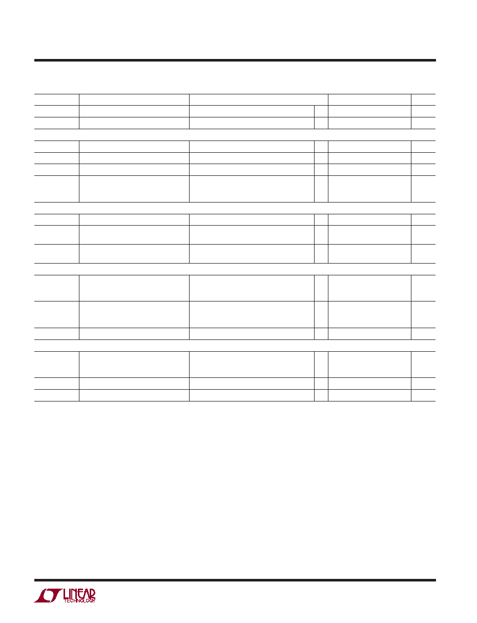
SYMBOL
PARAMETER
CONDITIONS
MIN
TYP
MAX
UNITS
tTMRDIS
Timer Discharge Time
CTMR = 1000pF, RTMR = 4.7k
l
40
120
ns
VTMRMAX
Timer Pin Clamp Voltage
CTMR = 1000pF, RTMR = 4.7k
2.5
V
Current Sense
ICS+
CS+ Input Current
VCS+ = 0V
l
±1
A
ICS–
CS– Input Current
VCS– = 0V
l
±1
A
VCSMAX
CS+ Pin Clamp Voltage
IIN = 5mA, VSYNC = –5V
11
V
VCS
Current Sense Threshold Voltage
VCS– = 0V
LTC3900E/LTC3900I (Note 5)
LTC3900H/LTC3900MP (Note 5)
l
7.5
3
1
10.5
13.5
18
20
mV
SYNC Input
ISYNC
SYNC Input Current
VSYNC = ±10V
l
±1
±10
A
VSYNCP
SYNC Input Positive Threshold
SYNC Positive Input Hysteresis
(Note 6)
l
1.0
1.4
0.2
1.8
V
VSYNCN
SYNC Input Negative Threshold
SYNC Negative Input Hysteresis
(Note 6)
l
–1.8
–1.4
0.2
–1.0
V
Driver Output
RONH
Driver Pull-Up Resistance
IOUT = –100mA
LTC3900E/LTC3900I
LTC3900H/LTC3900MP
l
0.9
1.2
1.6
2.0
Ω
RONL
Driver Pull-Down Resistance
IOUT = 100mA
LTC3900E/LTC3900I
LTC3900H/LTC3900MP
l
0.9
1.2
1.6
2.0
Ω
IPK
Driver Peak Output Current
(Note 6)
2
A
Switching Characteristics (Note 7)
td
SYNC Input to Driver Output Delay
CFG = CCG = 4700pF, VSYNC = ±5V
LTC3900E/LTC3900I
LTC3900H/LTC3900MP
l
60
120
150
ns
tSYNC
Minimum SYNC Pulse Width
VSYNC = ±5V
l
75
ns
tr, tf
Driver Rise/Fall Time
CFG = CCG = 4700pF, VSYNC = ±5V
15
ns
elecTrical characTerisTics The
l
denotes the specifications which apply over the specified operating
junction temperature range, otherwise specifications are at TA = 25°C. VCC = 5V unless otherwise specified. (Notes 2, 3)
Note 1: Stresses beyond those listed under Absolute Maximum Ratings
may cause permanent damage to the device. Exposure to any Absolute
Maximum Rating condition for extended periods may affect device
reliability and lifetime.
Note 2: The LTC3900 is tested under pulsed load conditions such that
TJ ≈ TA. The LTC3900E is guaranteed to meet performance specifications
from 0°C to 85°C operating junction temperature. Specifications over
the –40°C to 125°C operating junction temperature range are assured
by design, characterization and correlation with statistical process
controls. The LTC3900I is guaranteed over the –40°C to 125°C operating
junction temperature range. The LTC3900H is guaranteed over the full
–40°C to 150°C operating junction temperature range. The LTC3900MP
is guaranteed and tested over the full –55°C to 150°C operating junction
temperature range. High junction temperatures degrade operating
lifetimes; operating lifetime is derated for junction temperatures greater
than 125°C. Note that the maximum ambient temperature consistent
with these specifications is determined by specific operating conditions
in conjunction with board layout, the rated package thermal impedance
and other environmental factors. The junction temperature (TJ, in °C) is
calculated from the ambient temperature (TA, in °C) and power dissipation
(PD, in watts) according to the formula:
TJ = TA + (PD θJA), where θJA (in °C/W) is the package thermal
impedance.
Note 3: All currents into device pins are positive; all currents out of device
pins are negative. All voltages are referenced to ground unless otherwise
specified.
Note 4: Supply current in normal operation is dominated by the current
needed to charge and discharge the external MOSFET gates. This current
will vary with supply voltage, switching frequency and the external
MOSFETs used.
Note 5: The current sense comparator threshold has a 0.33%/°C
temperature coefficient (TC) to match the TC of the external MOSFET
RDS(ON).
Note 6: Guaranteed by design, not subject to test.
Note 7: Rise and fall times are measured using 10% and 90% levels. Delay
times are measured from ±1.4V at SYNC input to 20%/80% levels at the
driver output.
相关PDF资料 |
PDF描述 |
|---|---|
| LM336H-2.5 | 1-OUTPUT TWO TERM VOLTAGE REFERENCE, 2.49 V, MBCY3 |
| LPC48DP | 2-OUTPUT 75 W DC-DC REG PWR SUPPLY MODULE |
| LK1001-7EPD6TB1 | 1-OUTPUT 150 W AC-DC REG PWR SUPPLY MODULE |
| LS1001-7EPV2B1 | 1-OUTPUT AC-DC REG PWR SUPPLY MODULE |
| LS1001-7PD0 | 1-OUTPUT AC-DC REG PWR SUPPLY MODULE |
相关代理商/技术参数 |
参数描述 |
|---|---|
| LTC3900MPS8#PBF | 功能描述:IC DRIVER RECT SYNC CONV 8SOIC RoHS:是 类别:集成电路 (IC) >> PMIC - MOSFET,电桥驱动器 - 外部开关 系列:- 标准包装:5 系列:- 配置:低端 输入类型:非反相 延迟时间:600ns 电流 - 峰:12A 配置数:1 输出数:1 高端电压 - 最大(自引导启动):- 电源电压:14.2 V ~ 15.8 V 工作温度:-20°C ~ 60°C 安装类型:通孔 封装/外壳:21-SIP 模块 供应商设备封装:模块 包装:散装 配用:BG2A-NF-ND - KIT DEV BOARD FOR IGBT 其它名称:835-1063 |
| LTC3900MPS8#TRPBF | 功能描述:IC DRIVER RECT SYNC CONV 8SOIC RoHS:是 类别:集成电路 (IC) >> PMIC - MOSFET,电桥驱动器 - 外部开关 系列:- 标准包装:5 系列:- 配置:低端 输入类型:非反相 延迟时间:600ns 电流 - 峰:12A 配置数:1 输出数:1 高端电压 - 最大(自引导启动):- 电源电压:14.2 V ~ 15.8 V 工作温度:-20°C ~ 60°C 安装类型:通孔 封装/外壳:21-SIP 模块 供应商设备封装:模块 包装:散装 配用:BG2A-NF-ND - KIT DEV BOARD FOR IGBT 其它名称:835-1063 |
| LTC3901EGN | 功能描述:IC DRIVER RECT SYNC CONV 16SSOP RoHS:否 类别:集成电路 (IC) >> PMIC - MOSFET,电桥驱动器 - 外部开关 系列:- 标准包装:5 系列:- 配置:低端 输入类型:非反相 延迟时间:600ns 电流 - 峰:12A 配置数:1 输出数:1 高端电压 - 最大(自引导启动):- 电源电压:14.2 V ~ 15.8 V 工作温度:-20°C ~ 60°C 安装类型:通孔 封装/外壳:21-SIP 模块 供应商设备封装:模块 包装:散装 配用:BG2A-NF-ND - KIT DEV BOARD FOR IGBT 其它名称:835-1063 |
| LTC3901EGN#PBF | 功能描述:IC DRIVER RECT SYNC CONV 16SSOP RoHS:是 类别:集成电路 (IC) >> PMIC - MOSFET,电桥驱动器 - 外部开关 系列:- 标准包装:5 系列:- 配置:低端 输入类型:非反相 延迟时间:600ns 电流 - 峰:12A 配置数:1 输出数:1 高端电压 - 最大(自引导启动):- 电源电压:14.2 V ~ 15.8 V 工作温度:-20°C ~ 60°C 安装类型:通孔 封装/外壳:21-SIP 模块 供应商设备封装:模块 包装:散装 配用:BG2A-NF-ND - KIT DEV BOARD FOR IGBT 其它名称:835-1063 |
| LTC3901EGN#TR | 功能描述:IC DRIVER RECT SYNC CONV 16SSOP RoHS:否 类别:集成电路 (IC) >> PMIC - MOSFET,电桥驱动器 - 外部开关 系列:- 标准包装:5 系列:- 配置:低端 输入类型:非反相 延迟时间:600ns 电流 - 峰:12A 配置数:1 输出数:1 高端电压 - 最大(自引导启动):- 电源电压:14.2 V ~ 15.8 V 工作温度:-20°C ~ 60°C 安装类型:通孔 封装/外壳:21-SIP 模块 供应商设备封装:模块 包装:散装 配用:BG2A-NF-ND - KIT DEV BOARD FOR IGBT 其它名称:835-1063 |
发布紧急采购,3分钟左右您将得到回复。