- 您现在的位置:买卖IC网 > PDF目录80246 > LTC3900MPS8 (LINEAR TECHNOLOGY CORP) SWITCHING REGULATOR, PDSO8 PDF资料下载
参数资料
| 型号: | LTC3900MPS8 |
| 厂商: | LINEAR TECHNOLOGY CORP |
| 元件分类: | 稳压器 |
| 英文描述: | SWITCHING REGULATOR, PDSO8 |
| 封装: | PLASTIC, SOP-8 |
| 文件页数: | 19/20页 |
| 文件大小: | 277K |
| 代理商: | LTC3900MPS8 |
LTC3900
8
3900fb
applicaTions inForMaTion
ThetimercircuitandcurrentsensecomparatorinLTC3900
are used to prevent reverse current buildup in the output
inductor.
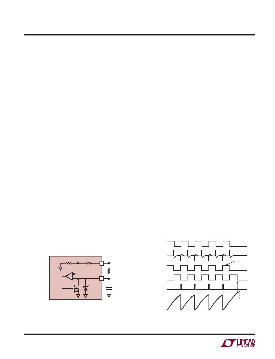
Timer
Figure 3 shows the LTC3900 timer internal and external
circuits. The timer operates by using an external R-C
charging network to program the time-out period. On
every negative transition at the SYNC input, the chip
generates a 200ns pulse to reset the timer cap. If the
SYNC signal is missing or incorrect, allowing the timer
cap voltage to go high, it shuts off both drivers once the
voltage reaches the time-out threshold. Figure 4 shows
the timer waveforms.
A typical forward converter cycle always turns on Q3
and Q4 alternately and the SYNC input should alternate
between positive and negative pulses. The LTC3900 timer
also includes sequential logic to monitor the SYNC input
sequence. If after one negative pulse, the SYNC compara-
tor receives another negative pulse, the LTC3900 will not
reset the timer cap. If no positive SYNC pulse appears,
both drivers are shut off once the timer times out. Once
positive pulses reappear the timer resets and the drivers
start switching again. This is to protect the external com-
ponents in situations where only negative SYNC pulse is
present and FG output remains high. Figure 5 shows the
timer waveforms with incorrect SYNC pulses.
The LTC3900 has two separate SYNC comparators (S+ and
S–intheBlockDiagram)todetectthepositiveandnegative
pulses. The threshold voltages of both comparators are
Figure 3. Timer Circuit
ZTMR
RTMR
CTMR
7
3900 F03
TMR
4
R1
R2
VCC
TIMEOUT
TIMER
RESET
designed to be of the same magnitude (1.4V typical) but
opposite in polarity. In some situations, for example dur-
ing power up or power down, the SYNC pulse magnitude
may be low, slightly higher or lower than the threshold of
the comparators. This can cause only one of the SYNC
comparators to trip. This also appears as incorrect SYNC
pulse and the timer will not reset.
The timeout period is determined by the external RTMR
and CTMR values and is independent of the VCC voltage.
This is achieved by making the timeout threshold a ratio
of VCC. The ratio is 0.2x, set internally by R1 and R2 (see
Figure 3). The timeout period should be programmed to
be around one period of the primary switching frequency
using the following formula:
TIMEOUT = 0.2 RTMR CTMR + 0.27E-6
To reduce error in the timeout setting due to the discharge
time, select CTMR between 100pF and 1000pF. Start with a
CTMRaround 470pF and then calculate the required RTMR.
CTMRshouldbeplacedascloseaspossibletotheLTC3900
with minimum PCB trace between CTMR, the TIMER pin
and GND. This is to reduce any ringing caused by the PCB
trace inductance when CTMR discharges. This ringing may
introduce error to the timeout setting.
The timer input also includes a current sinking clamp
circuit (ZTMR in Figure 3) that clamps this pin to about
0.5 VCC if there is missing SYNC/timer reset pulse. This
clamp circuit prevents the timer cap from getting fully
charged up to the rail, which results in a longer discharge
SYNC
FG
CG
TIMER RESET
(INTERNAL)
TIMER
SG
TIMEOUT
THRESHOLD
LAST
PULSE
3900 F04
Figure 4. Timer Waveforms
相关PDF资料 |
PDF描述 |
|---|---|
| LM336H-2.5 | 1-OUTPUT TWO TERM VOLTAGE REFERENCE, 2.49 V, MBCY3 |
| LPC48DP | 2-OUTPUT 75 W DC-DC REG PWR SUPPLY MODULE |
| LK1001-7EPD6TB1 | 1-OUTPUT 150 W AC-DC REG PWR SUPPLY MODULE |
| LS1001-7EPV2B1 | 1-OUTPUT AC-DC REG PWR SUPPLY MODULE |
| LS1001-7PD0 | 1-OUTPUT AC-DC REG PWR SUPPLY MODULE |
相关代理商/技术参数 |
参数描述 |
|---|---|
| LTC3900MPS8#PBF | 功能描述:IC DRIVER RECT SYNC CONV 8SOIC RoHS:是 类别:集成电路 (IC) >> PMIC - MOSFET,电桥驱动器 - 外部开关 系列:- 标准包装:5 系列:- 配置:低端 输入类型:非反相 延迟时间:600ns 电流 - 峰:12A 配置数:1 输出数:1 高端电压 - 最大(自引导启动):- 电源电压:14.2 V ~ 15.8 V 工作温度:-20°C ~ 60°C 安装类型:通孔 封装/外壳:21-SIP 模块 供应商设备封装:模块 包装:散装 配用:BG2A-NF-ND - KIT DEV BOARD FOR IGBT 其它名称:835-1063 |
| LTC3900MPS8#TRPBF | 功能描述:IC DRIVER RECT SYNC CONV 8SOIC RoHS:是 类别:集成电路 (IC) >> PMIC - MOSFET,电桥驱动器 - 外部开关 系列:- 标准包装:5 系列:- 配置:低端 输入类型:非反相 延迟时间:600ns 电流 - 峰:12A 配置数:1 输出数:1 高端电压 - 最大(自引导启动):- 电源电压:14.2 V ~ 15.8 V 工作温度:-20°C ~ 60°C 安装类型:通孔 封装/外壳:21-SIP 模块 供应商设备封装:模块 包装:散装 配用:BG2A-NF-ND - KIT DEV BOARD FOR IGBT 其它名称:835-1063 |
| LTC3901EGN | 功能描述:IC DRIVER RECT SYNC CONV 16SSOP RoHS:否 类别:集成电路 (IC) >> PMIC - MOSFET,电桥驱动器 - 外部开关 系列:- 标准包装:5 系列:- 配置:低端 输入类型:非反相 延迟时间:600ns 电流 - 峰:12A 配置数:1 输出数:1 高端电压 - 最大(自引导启动):- 电源电压:14.2 V ~ 15.8 V 工作温度:-20°C ~ 60°C 安装类型:通孔 封装/外壳:21-SIP 模块 供应商设备封装:模块 包装:散装 配用:BG2A-NF-ND - KIT DEV BOARD FOR IGBT 其它名称:835-1063 |
| LTC3901EGN#PBF | 功能描述:IC DRIVER RECT SYNC CONV 16SSOP RoHS:是 类别:集成电路 (IC) >> PMIC - MOSFET,电桥驱动器 - 外部开关 系列:- 标准包装:5 系列:- 配置:低端 输入类型:非反相 延迟时间:600ns 电流 - 峰:12A 配置数:1 输出数:1 高端电压 - 最大(自引导启动):- 电源电压:14.2 V ~ 15.8 V 工作温度:-20°C ~ 60°C 安装类型:通孔 封装/外壳:21-SIP 模块 供应商设备封装:模块 包装:散装 配用:BG2A-NF-ND - KIT DEV BOARD FOR IGBT 其它名称:835-1063 |
| LTC3901EGN#TR | 功能描述:IC DRIVER RECT SYNC CONV 16SSOP RoHS:否 类别:集成电路 (IC) >> PMIC - MOSFET,电桥驱动器 - 外部开关 系列:- 标准包装:5 系列:- 配置:低端 输入类型:非反相 延迟时间:600ns 电流 - 峰:12A 配置数:1 输出数:1 高端电压 - 最大(自引导启动):- 电源电压:14.2 V ~ 15.8 V 工作温度:-20°C ~ 60°C 安装类型:通孔 封装/外壳:21-SIP 模块 供应商设备封装:模块 包装:散装 配用:BG2A-NF-ND - KIT DEV BOARD FOR IGBT 其它名称:835-1063 |
发布紧急采购,3分钟左右您将得到回复。