- 您现在的位置:买卖IC网 > PDF目录80246 > LTC3900MPS8 (LINEAR TECHNOLOGY CORP) SWITCHING REGULATOR, PDSO8 PDF资料下载
参数资料
| 型号: | LTC3900MPS8 |
| 厂商: | LINEAR TECHNOLOGY CORP |
| 元件分类: | 稳压器 |
| 英文描述: | SWITCHING REGULATOR, PDSO8 |
| 封装: | PLASTIC, SOP-8 |
| 文件页数: | 18/20页 |
| 文件大小: | 277K |
| 代理商: | LTC3900MPS8 |
LTC3900
7
3900fb
applicaTions inForMaTion
Overview
In a typical forward converter topology, a power trans-
former is used to provide the functions of input/output
isolation and voltage step-down to achieve the required
low output voltage. Schottky diodes are often used on
the secondary-side to provide rectification. Schottky
diodes, though easy to use, result in a loss of efficiency
due to relatively high voltage drops. To improve efficiency,
synchronousoutputrectifiersutilizingN-channelMOSFETs
can be used instead of Schottky diodes. The LTC3900
provides all of the necessary functions required to drive
the synchronous rectifier MOSFETs.
Figure 1 shows a simplified forward converter application.
T1 is the power transformer; Q1 is the primary-side power
transistor driven by the primary controller, LT1952 output
(OUT).ThepulsetransformerT2providessynchronization
andisdrivenbyLT1952synchronizationsignal,SOUTorSG
from the primary controller. Q3 and Q4 are secondary-side
synchronous switches driven by the LTC3900’s FG and CG
output. Inductor LO and capacitor COUT form the output
filter to provide a steady DC output voltage for the load.
Also shown in Figure 1 is the feedback path from VOUT
throughtheoptocouplerdriverLT4430andanoptocoupler,
back to the primary controller to regulate VOUT.
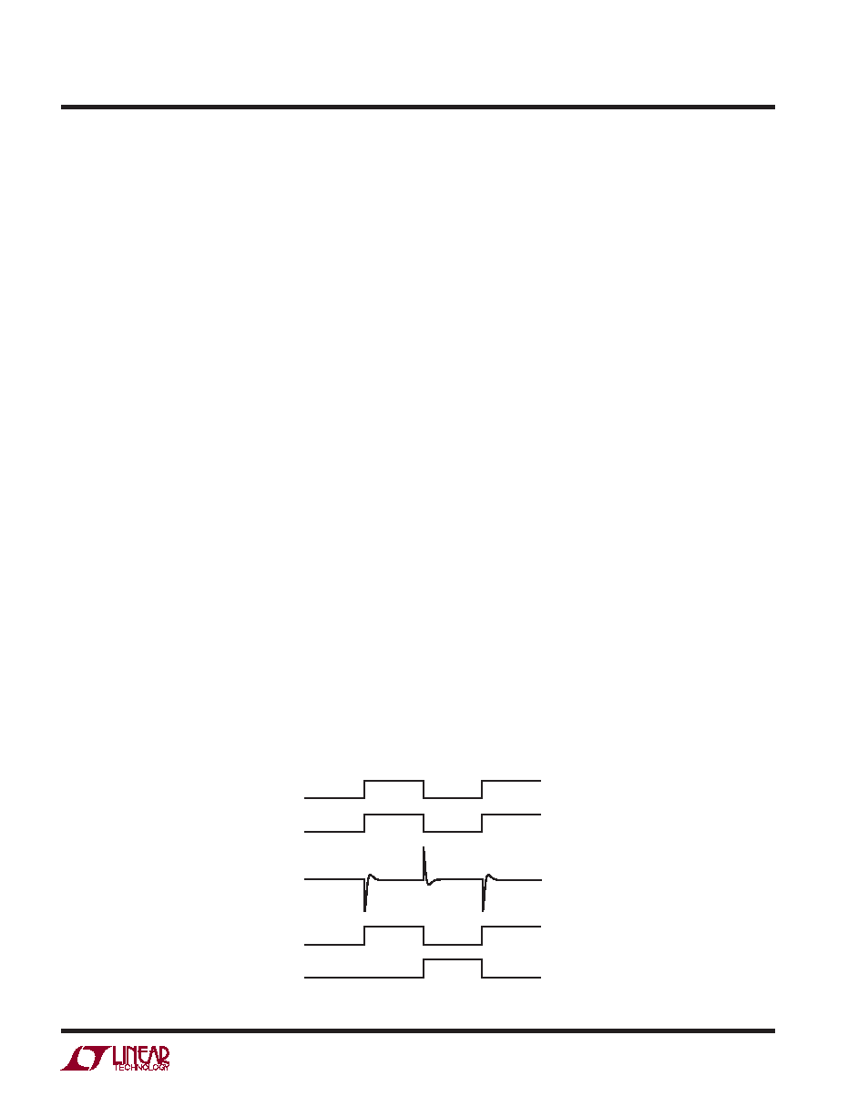
Each full cycle of the forward converter operation con-
sists of two periods. In the first period, Q1 turns on and
the primary-side delivers power to the load through T1.
SG goes high and T2 generates a negative pulse at the
LTC3900 SYNC input. The LTC3900 forces FG to turn on
and CG to turn off, Q3 conducts. Current flows to the
load through Q3, T1 and LO. In the next period, Q1 turns
off, SG goes low and T2 generates a positive pulse at the
LTC3900 SYNC input. The LTC3900 forces FG to turn off
and CG to turn on, Q4 conducts. Current continues to
flow to the load through Q4 and LO. Figure 2 shows the
LTC3900 synchronization waveforms.
External MOSFET Protection
Aprogrammabletimerandadifferentialinputcurrentsense
comparator are included in the LTC3900 for protection
of the external MOSFET during power down and Burst
Mode operation. The chip also shuts off the MOSFETs
if VCC < 4.1V.
Whentheprimarycontrollerispoweringdown,theprimary
controller shuts down first and the LTC3900 continues to
operate for a while by drawing power from the VCCbypass
cap, CVCC. The SG signal stops switching and there is no
SYNC pulse to the LTC3900. The LTC3900 keeps one of
the drivers turned on depending on the polarity of the
last SYNC pulse. If the last SYNC pulse is positive, CG
will remain high and the catch MOSFET, Q4 will stay on.
The inductor current will start falling down to zero and
continue going in the negative direction due to the voltage
that is still present across the output capacitor (the current
now flows from COUT back to LO). If Q4 is turned off while
the inductor current is negative, the inductor current will
produce high voltage across Q4, resulting in a MOSFET
avalanche. Depending on the amount of energy stored in
the inductor, this avalanche energy may damage Q4.
Figure 2. Synchronization Waveforms
GATE
(OUT)
SG
(SOUT)
SYNC
FG
CG
3900 F02
相关PDF资料 |
PDF描述 |
|---|---|
| LM336H-2.5 | 1-OUTPUT TWO TERM VOLTAGE REFERENCE, 2.49 V, MBCY3 |
| LPC48DP | 2-OUTPUT 75 W DC-DC REG PWR SUPPLY MODULE |
| LK1001-7EPD6TB1 | 1-OUTPUT 150 W AC-DC REG PWR SUPPLY MODULE |
| LS1001-7EPV2B1 | 1-OUTPUT AC-DC REG PWR SUPPLY MODULE |
| LS1001-7PD0 | 1-OUTPUT AC-DC REG PWR SUPPLY MODULE |
相关代理商/技术参数 |
参数描述 |
|---|---|
| LTC3900MPS8#PBF | 功能描述:IC DRIVER RECT SYNC CONV 8SOIC RoHS:是 类别:集成电路 (IC) >> PMIC - MOSFET,电桥驱动器 - 外部开关 系列:- 标准包装:5 系列:- 配置:低端 输入类型:非反相 延迟时间:600ns 电流 - 峰:12A 配置数:1 输出数:1 高端电压 - 最大(自引导启动):- 电源电压:14.2 V ~ 15.8 V 工作温度:-20°C ~ 60°C 安装类型:通孔 封装/外壳:21-SIP 模块 供应商设备封装:模块 包装:散装 配用:BG2A-NF-ND - KIT DEV BOARD FOR IGBT 其它名称:835-1063 |
| LTC3900MPS8#TRPBF | 功能描述:IC DRIVER RECT SYNC CONV 8SOIC RoHS:是 类别:集成电路 (IC) >> PMIC - MOSFET,电桥驱动器 - 外部开关 系列:- 标准包装:5 系列:- 配置:低端 输入类型:非反相 延迟时间:600ns 电流 - 峰:12A 配置数:1 输出数:1 高端电压 - 最大(自引导启动):- 电源电压:14.2 V ~ 15.8 V 工作温度:-20°C ~ 60°C 安装类型:通孔 封装/外壳:21-SIP 模块 供应商设备封装:模块 包装:散装 配用:BG2A-NF-ND - KIT DEV BOARD FOR IGBT 其它名称:835-1063 |
| LTC3901EGN | 功能描述:IC DRIVER RECT SYNC CONV 16SSOP RoHS:否 类别:集成电路 (IC) >> PMIC - MOSFET,电桥驱动器 - 外部开关 系列:- 标准包装:5 系列:- 配置:低端 输入类型:非反相 延迟时间:600ns 电流 - 峰:12A 配置数:1 输出数:1 高端电压 - 最大(自引导启动):- 电源电压:14.2 V ~ 15.8 V 工作温度:-20°C ~ 60°C 安装类型:通孔 封装/外壳:21-SIP 模块 供应商设备封装:模块 包装:散装 配用:BG2A-NF-ND - KIT DEV BOARD FOR IGBT 其它名称:835-1063 |
| LTC3901EGN#PBF | 功能描述:IC DRIVER RECT SYNC CONV 16SSOP RoHS:是 类别:集成电路 (IC) >> PMIC - MOSFET,电桥驱动器 - 外部开关 系列:- 标准包装:5 系列:- 配置:低端 输入类型:非反相 延迟时间:600ns 电流 - 峰:12A 配置数:1 输出数:1 高端电压 - 最大(自引导启动):- 电源电压:14.2 V ~ 15.8 V 工作温度:-20°C ~ 60°C 安装类型:通孔 封装/外壳:21-SIP 模块 供应商设备封装:模块 包装:散装 配用:BG2A-NF-ND - KIT DEV BOARD FOR IGBT 其它名称:835-1063 |
| LTC3901EGN#TR | 功能描述:IC DRIVER RECT SYNC CONV 16SSOP RoHS:否 类别:集成电路 (IC) >> PMIC - MOSFET,电桥驱动器 - 外部开关 系列:- 标准包装:5 系列:- 配置:低端 输入类型:非反相 延迟时间:600ns 电流 - 峰:12A 配置数:1 输出数:1 高端电压 - 最大(自引导启动):- 电源电压:14.2 V ~ 15.8 V 工作温度:-20°C ~ 60°C 安装类型:通孔 封装/外壳:21-SIP 模块 供应商设备封装:模块 包装:散装 配用:BG2A-NF-ND - KIT DEV BOARD FOR IGBT 其它名称:835-1063 |
发布紧急采购,3分钟左右您将得到回复。