- 您现在的位置:买卖IC网 > PDF目录80246 > LTC3900MPS8 (LINEAR TECHNOLOGY CORP) SWITCHING REGULATOR, PDSO8 PDF资料下载
参数资料
| 型号: | LTC3900MPS8 |
| 厂商: | LINEAR TECHNOLOGY CORP |
| 元件分类: | 稳压器 |
| 英文描述: | SWITCHING REGULATOR, PDSO8 |
| 封装: | PLASTIC, SOP-8 |
| 文件页数: | 3/20页 |
| 文件大小: | 277K |
| 代理商: | LTC3900MPS8 |
LTC3900
11
3900fb
applicaTions inForMaTion
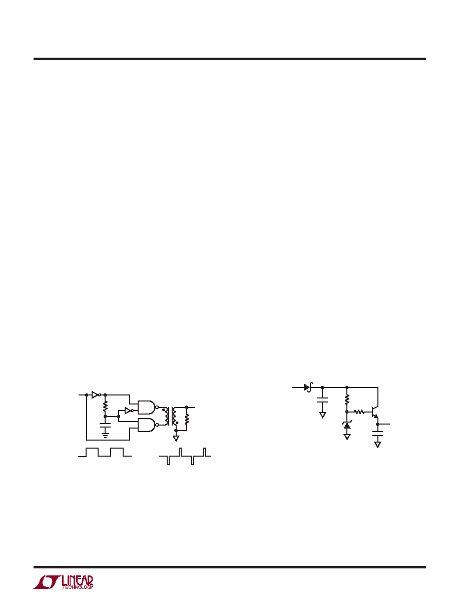
An alternative method of generating the SYNC pulse is
shown in Figure 8. This circuit produces square SYNC
pulses with amplitude dependent on the logic supply
voltage. The SYNC pulse width can be adjusted with R1
and C1 without affecting the pulse amplitude.
Fornonisolatedapplications,theSYNCinputcanbedriven
directly by a bipolar square pulse. To reduce the propa-
gation delay, make the positive and negative magnitude
of the square wave much greater than the ±1.4V SYNC
threshold.
VCC Regulator
The VCC supply for the LTC3900 can be generated by peak
rectifying the transformer secondary winding as shown
in Figure 9. The Zener diode DZ sets the output voltage to
(VZ – 0.7V). A resistor, RB (on the order of a few hundred
ohms), in series with the base of QREG may be required
to surpress high frequency oscillations depending on
QREG’s selection.
The LTC3900 has an UVLO detector that pulls the drivers
output low if VCC < 4.1V. The UVLO detector has 0.5V of
hysteresis to prevent chattering.
In a typical forward converter, the secondary-side circuits
have no power until the primary-side controller starts
operating. Since the power for biasing the LTC3900 is
derived from the power transformer T1, the LTC3900 will
initially remain off. During that period (VCC < 4.1V), the
output rectifier MOSFETs Q3 and Q4 will remain off and
the MOSFETs body diodes will conduct. The MOSFETs
may experience very high power dissipation due to a high
voltage drop in the body diodes. To prevent MOSFET dam-
age, VCC voltage greater than 4.1V should be provided
quickly. The VCC supply circuit shown in Figure 9 will pro-
vide power for the LTC3900 within the first few switching
pulses of the primary controller, preventing overheating
of the MOSFETs.
MOSFET Selection
TherequiredMOSFETRDS(ON)shouldbedeterminedbased
on allowable power dissipation and maximum required
output current.
Thebodydiodesconductduringthepower-upphase,when
the LTC3900 VCC supply is ramping up. The CG and FG
signals stay low and the inductor current flows through
the body diodes. The body diodes must be able to handle
the load current during start-up until VCC reaches 4.1V.
The LTC3900 drivers dissipate power when switching
MOSFETs. The power dissipation increases with switch-
ing frequency, VCC and size of the MOSFETs. To calculate
Figure 9. VCC Regulator
Figure 8. Symmetrical SYNC Drive
RSYNC
470
T2
LTC3900
SYNC
3900 F08
74HC14
74HC132
R1
470
C1
220pF
SYNC
SG
PRIMARY
CONTROLLER
SG
3900 F09
D3
MBR0540
T1
SECONDARY
WINDING
0.1F
RZ
2k
RB
10
QREG
BCX55
CVCC
4.7F
VCC
DZ
7.5V
相关PDF资料 |
PDF描述 |
|---|---|
| LM336H-2.5 | 1-OUTPUT TWO TERM VOLTAGE REFERENCE, 2.49 V, MBCY3 |
| LPC48DP | 2-OUTPUT 75 W DC-DC REG PWR SUPPLY MODULE |
| LK1001-7EPD6TB1 | 1-OUTPUT 150 W AC-DC REG PWR SUPPLY MODULE |
| LS1001-7EPV2B1 | 1-OUTPUT AC-DC REG PWR SUPPLY MODULE |
| LS1001-7PD0 | 1-OUTPUT AC-DC REG PWR SUPPLY MODULE |
相关代理商/技术参数 |
参数描述 |
|---|---|
| LTC3900MPS8#PBF | 功能描述:IC DRIVER RECT SYNC CONV 8SOIC RoHS:是 类别:集成电路 (IC) >> PMIC - MOSFET,电桥驱动器 - 外部开关 系列:- 标准包装:5 系列:- 配置:低端 输入类型:非反相 延迟时间:600ns 电流 - 峰:12A 配置数:1 输出数:1 高端电压 - 最大(自引导启动):- 电源电压:14.2 V ~ 15.8 V 工作温度:-20°C ~ 60°C 安装类型:通孔 封装/外壳:21-SIP 模块 供应商设备封装:模块 包装:散装 配用:BG2A-NF-ND - KIT DEV BOARD FOR IGBT 其它名称:835-1063 |
| LTC3900MPS8#TRPBF | 功能描述:IC DRIVER RECT SYNC CONV 8SOIC RoHS:是 类别:集成电路 (IC) >> PMIC - MOSFET,电桥驱动器 - 外部开关 系列:- 标准包装:5 系列:- 配置:低端 输入类型:非反相 延迟时间:600ns 电流 - 峰:12A 配置数:1 输出数:1 高端电压 - 最大(自引导启动):- 电源电压:14.2 V ~ 15.8 V 工作温度:-20°C ~ 60°C 安装类型:通孔 封装/外壳:21-SIP 模块 供应商设备封装:模块 包装:散装 配用:BG2A-NF-ND - KIT DEV BOARD FOR IGBT 其它名称:835-1063 |
| LTC3901EGN | 功能描述:IC DRIVER RECT SYNC CONV 16SSOP RoHS:否 类别:集成电路 (IC) >> PMIC - MOSFET,电桥驱动器 - 外部开关 系列:- 标准包装:5 系列:- 配置:低端 输入类型:非反相 延迟时间:600ns 电流 - 峰:12A 配置数:1 输出数:1 高端电压 - 最大(自引导启动):- 电源电压:14.2 V ~ 15.8 V 工作温度:-20°C ~ 60°C 安装类型:通孔 封装/外壳:21-SIP 模块 供应商设备封装:模块 包装:散装 配用:BG2A-NF-ND - KIT DEV BOARD FOR IGBT 其它名称:835-1063 |
| LTC3901EGN#PBF | 功能描述:IC DRIVER RECT SYNC CONV 16SSOP RoHS:是 类别:集成电路 (IC) >> PMIC - MOSFET,电桥驱动器 - 外部开关 系列:- 标准包装:5 系列:- 配置:低端 输入类型:非反相 延迟时间:600ns 电流 - 峰:12A 配置数:1 输出数:1 高端电压 - 最大(自引导启动):- 电源电压:14.2 V ~ 15.8 V 工作温度:-20°C ~ 60°C 安装类型:通孔 封装/外壳:21-SIP 模块 供应商设备封装:模块 包装:散装 配用:BG2A-NF-ND - KIT DEV BOARD FOR IGBT 其它名称:835-1063 |
| LTC3901EGN#TR | 功能描述:IC DRIVER RECT SYNC CONV 16SSOP RoHS:否 类别:集成电路 (IC) >> PMIC - MOSFET,电桥驱动器 - 外部开关 系列:- 标准包装:5 系列:- 配置:低端 输入类型:非反相 延迟时间:600ns 电流 - 峰:12A 配置数:1 输出数:1 高端电压 - 最大(自引导启动):- 电源电压:14.2 V ~ 15.8 V 工作温度:-20°C ~ 60°C 安装类型:通孔 封装/外壳:21-SIP 模块 供应商设备封装:模块 包装:散装 配用:BG2A-NF-ND - KIT DEV BOARD FOR IGBT 其它名称:835-1063 |
发布紧急采购,3分钟左右您将得到回复。