- 您现在的位置:买卖IC网 > PDF目录80246 > LTC3900MPS8 (LINEAR TECHNOLOGY CORP) SWITCHING REGULATOR, PDSO8 PDF资料下载
参数资料
| 型号: | LTC3900MPS8 |
| 厂商: | LINEAR TECHNOLOGY CORP |
| 元件分类: | 稳压器 |
| 英文描述: | SWITCHING REGULATOR, PDSO8 |
| 封装: | PLASTIC, SOP-8 |
| 文件页数: | 20/20页 |
| 文件大小: | 277K |
| 代理商: | LTC3900MPS8 |
LTC3900
9
3900fb
applicaTions inForMaTion
time. The current sinking capability of the circuit is around
1mA. The timeout function can be disabled by connecting
the timer pin to GND.
Current Sense
The differential input current sense comparator is used
for sensing the voltage across the drain-to-source termi-
nals of Q4 through the CS+ and CS– pins. If the inductor
current reverses into the Q4 causing CS+ to rise above
CS– by more than 10.5mV, the LTC3900 pulls CG low. This
comparator is used to prevent inductor reverse current
buildupduringpowerdownorBurstModeoperation,which
may cause damage to the MOSFET. The 10.5mV input
threshold has a positive temperature coefficient, which
closely matches the TC of the external MOSFET RDS(ON).
The current sense comparator is only active 250ns after
CG goes high; this is to avoid any ringing immediately
after Q4 is switched on.
Under light load conditions, if the inductor average cur-
rent is less than half of its peak-to-peak ripple current,
the inductor current will reverse into Q4 during a portion
of the switching cycle, forcing CS+ to rise above CS–.
The current sense comparator input threshold is set at
10.5mV to prevent tripping under light load conditions.
If the product of the inductor negative peak current and
MOSFET RDS(ON) is higher than 10.5mV, the LTC3900 will
operate in discontinuous current mode. Figure 6 shows
the LTC3900 operating in discontinuous current mode;
the CG output goes low before the next negative SYNC
pulse, as soon as the inductor current becomes negative.
Discontinuous current mode is sometimes undesirable.
To disable discontinuous current mode operation, add a
resistor divider, RCS1 and RCS2 at the CS+ pin to increase
the 10.5mV threshold so that the LTC3900 operates in
continuous mode at no load.
The LTC3900 CS+ pin has an internal current sinking
clamp circuit (ZCS in the Block Diagram) that clamps the
pin to 11V. The clamp circuit is to be used together with
the external series resistor, RCS1 to protect the CS+ pin
from high Q4 drain voltage in the power transfer cycle.
During the power transfer cycle, Q4 is off, the drain volt-
age of Q4 is determined by the primary input voltage and
the transformer turns ratio. This voltage can be high and
may damage the LTC3900 if CS+ is connected directly to
the drain of Q4. The current sinking capability of the clamp
circuit is 5mA minimum.
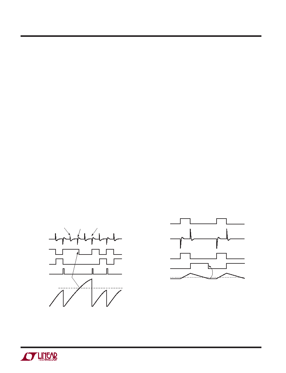
SYNC
FG
CG
TIMER RESET
(INTERNAL)
TIMER
TIMEOUT
THRESHOLD
3900 F05
TIMEOUT
MISSING/LOW
POSITIVE
SYNC PULSE
TIMER RESET AFTER
RECEIVING POSITIVE
SYNC PULSE
TIMER DO NOT RESET
AT SECOND NEGATIVE
SYNC PULSE
Figure 5. Timer Waveforms with Incorrect SYNC Pulses
SG
SYNC
FG
CG
3900 F06a
INDUCTOR
CURRENT
0A
CURRENT SENSE
COMPARATOR TRIP
Figure 6a. Discontinuous Current Mode Operation at No Load
相关PDF资料 |
PDF描述 |
|---|---|
| LM336H-2.5 | 1-OUTPUT TWO TERM VOLTAGE REFERENCE, 2.49 V, MBCY3 |
| LPC48DP | 2-OUTPUT 75 W DC-DC REG PWR SUPPLY MODULE |
| LK1001-7EPD6TB1 | 1-OUTPUT 150 W AC-DC REG PWR SUPPLY MODULE |
| LS1001-7EPV2B1 | 1-OUTPUT AC-DC REG PWR SUPPLY MODULE |
| LS1001-7PD0 | 1-OUTPUT AC-DC REG PWR SUPPLY MODULE |
相关代理商/技术参数 |
参数描述 |
|---|---|
| LTC3900MPS8#PBF | 功能描述:IC DRIVER RECT SYNC CONV 8SOIC RoHS:是 类别:集成电路 (IC) >> PMIC - MOSFET,电桥驱动器 - 外部开关 系列:- 标准包装:5 系列:- 配置:低端 输入类型:非反相 延迟时间:600ns 电流 - 峰:12A 配置数:1 输出数:1 高端电压 - 最大(自引导启动):- 电源电压:14.2 V ~ 15.8 V 工作温度:-20°C ~ 60°C 安装类型:通孔 封装/外壳:21-SIP 模块 供应商设备封装:模块 包装:散装 配用:BG2A-NF-ND - KIT DEV BOARD FOR IGBT 其它名称:835-1063 |
| LTC3900MPS8#TRPBF | 功能描述:IC DRIVER RECT SYNC CONV 8SOIC RoHS:是 类别:集成电路 (IC) >> PMIC - MOSFET,电桥驱动器 - 外部开关 系列:- 标准包装:5 系列:- 配置:低端 输入类型:非反相 延迟时间:600ns 电流 - 峰:12A 配置数:1 输出数:1 高端电压 - 最大(自引导启动):- 电源电压:14.2 V ~ 15.8 V 工作温度:-20°C ~ 60°C 安装类型:通孔 封装/外壳:21-SIP 模块 供应商设备封装:模块 包装:散装 配用:BG2A-NF-ND - KIT DEV BOARD FOR IGBT 其它名称:835-1063 |
| LTC3901EGN | 功能描述:IC DRIVER RECT SYNC CONV 16SSOP RoHS:否 类别:集成电路 (IC) >> PMIC - MOSFET,电桥驱动器 - 外部开关 系列:- 标准包装:5 系列:- 配置:低端 输入类型:非反相 延迟时间:600ns 电流 - 峰:12A 配置数:1 输出数:1 高端电压 - 最大(自引导启动):- 电源电压:14.2 V ~ 15.8 V 工作温度:-20°C ~ 60°C 安装类型:通孔 封装/外壳:21-SIP 模块 供应商设备封装:模块 包装:散装 配用:BG2A-NF-ND - KIT DEV BOARD FOR IGBT 其它名称:835-1063 |
| LTC3901EGN#PBF | 功能描述:IC DRIVER RECT SYNC CONV 16SSOP RoHS:是 类别:集成电路 (IC) >> PMIC - MOSFET,电桥驱动器 - 外部开关 系列:- 标准包装:5 系列:- 配置:低端 输入类型:非反相 延迟时间:600ns 电流 - 峰:12A 配置数:1 输出数:1 高端电压 - 最大(自引导启动):- 电源电压:14.2 V ~ 15.8 V 工作温度:-20°C ~ 60°C 安装类型:通孔 封装/外壳:21-SIP 模块 供应商设备封装:模块 包装:散装 配用:BG2A-NF-ND - KIT DEV BOARD FOR IGBT 其它名称:835-1063 |
| LTC3901EGN#TR | 功能描述:IC DRIVER RECT SYNC CONV 16SSOP RoHS:否 类别:集成电路 (IC) >> PMIC - MOSFET,电桥驱动器 - 外部开关 系列:- 标准包装:5 系列:- 配置:低端 输入类型:非反相 延迟时间:600ns 电流 - 峰:12A 配置数:1 输出数:1 高端电压 - 最大(自引导启动):- 电源电压:14.2 V ~ 15.8 V 工作温度:-20°C ~ 60°C 安装类型:通孔 封装/外壳:21-SIP 模块 供应商设备封装:模块 包装:散装 配用:BG2A-NF-ND - KIT DEV BOARD FOR IGBT 其它名称:835-1063 |
发布紧急采购,3分钟左右您将得到回复。