- 您现在的位置:买卖IC网 > PDF目录9218 > LTC6946IUFD-3#PBF (Linear Technology)IC INTEGER-N PLL W/VCO 28-QFN PDF资料下载
参数资料
| 型号: | LTC6946IUFD-3#PBF |
| 厂商: | Linear Technology |
| 文件页数: | 9/30页 |
| 文件大小: | 0K |
| 描述: | IC INTEGER-N PLL W/VCO 28-QFN |
| 软件下载: | PLLWizard™ PLLWizard™, with .NET 2.0 installer |
| 标准包装: | 73 |
| 类型: | 时钟/频率合成器(RF/IF),分数-N,整数-N, |
| PLL: | 是 |
| 输入: | 时钟 |
| 输出: | 时钟 |
| 电路数: | 1 |
| 比率 - 输入:输出: | 1:1 |
| 差分 - 输入:输出: | 是/是 |
| 频率 - 最大: | 5.79GHz |
| 除法器/乘法器: | 是/是 |
| 电源电压: | 3.15 V ~ 5.25 V |
| 工作温度: | -40°C ~ 105°C |
| 安装类型: | 表面贴装 |
| 封装/外壳: | 28-WFQFN 裸露焊盘 |
| 供应商设备封装: | 28-QFN(4x5) |
| 包装: | 管件 |
第1页第2页第3页第4页第5页第6页第7页第8页当前第9页第10页第11页第12页第13页第14页第15页第16页第17页第18页第19页第20页第21页第22页第23页第24页第25页第26页第27页第28页第29页第30页
LTC6946
17
6946fa
OPERATION
SERIAL PORT
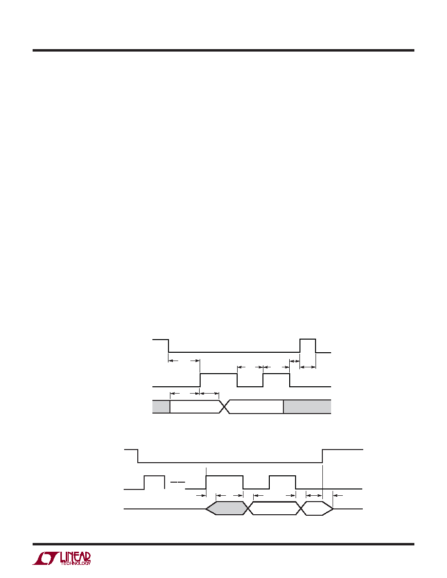
The SPI-compatible serial port provides control and
monitoring functionality. A configurable status output,
STAT, gives additional instant monitoring.
Communication Sequence
The serial bus is comprised of CS, SCLK, SDI and SDO.
Data transfers to the part are accomplished by the serial bus
master device first taking CS low to enable the LTC6946’s
port. Input data applied on SDI is clocked on the rising edge
of SCLK, with all transfers MSB first. The communication
burst is terminated by the serial bus master returning CS
high. See Figure 7 for details.
Data is read from the part during a communication burst
using SDO. Readback may be multidrop (more than one
LTC6946 connected in parallel on the serial bus), as SDO
is three-stated (Hi-Z) when CS = 1, or when data is not
being read from the part. If the LTC6946 is not used in
a multidrop configuration, or if the serial port master is
not capable of setting the SDO line level between read
sequences, it is recommended to attach a high value
resistor of greater than 200k between SDO and GND to
ensure the line returns to a known level during Hi-Z states.
See Figure 8 for details.
Single Byte Transfers
The serial port is arranged as a simple memory map, with
status and control available in 12, byte-wide registers. All
data bursts are comprised of at least two bytes. The 7 most
significant bits of the first byte are the register address,
with an LSB of 1 indicating a read from the part, and LSB
of 0 indicating a write to the part. The subsequent byte,
or bytes, is data from/to the specified register address.
See Figure 9 for an example of a detailed write sequence,
and Figure 10 for a read sequence.
Figure 11 shows an example of two write communication
bursts. The first byte of the first burst sent from the serial
bus master on SDI contains the destination register address
(Addr0) and an LSB of “0” indicating a write. The next byte
is the data intended for the register at address Addr0. CS is
then taken high to terminate the transfer. The first byte of
the second burst contains the destination register address
(Addr1) and an LSB indicating a write. The next byte on
SDI is the data intended for the register at address Addr1.
CS is then taken high to terminate the transfer.
MASTER–CS
MASTER–SCLK
tCSS
tCS
tCH
DATA
6946 F07
tCKL
tCKH
tCSS
tCSH
MASTER–SDI
MASTER–CS
MASTER–SCLK
LTC6946–SDO
Hi-Z
6946 F08
8TH CLOCK
DATA
tDO
Figure 7. Serial Port Write Timing Diagram
Figure 8. Serial Port Read Timing Diagram
相关PDF资料 |
PDF描述 |
|---|---|
| X9429WV14IZ-2.7 | IC XDCP SGL 64-TAP 10K 14-TSSOP |
| LTC6946IUFD-2#PBF | IC INTEGER-N PLL W/VCO 28-QFN |
| VI-B44-IU-B1 | CONVERTER MOD DC/DC 48V 200W |
| SY89429AJZ | IC SYNTHESIZER FREQ PROGR 28PLCC |
| SY58038UMY TR | IC MUX 8:1 PREC 1:2 LVPECL 44MLF |
相关代理商/技术参数 |
参数描述 |
|---|---|
| LTC6946-x | 制造商:LINER 制造商全称:Linear Technology 功能描述:16-Bit, 20Msps Low Noise Dual ADC |
| LTC694C | 制造商:LINER 制造商全称:Linear Technology 功能描述:Microprocessor Supervisory Circuits |
| LTC694C-3.3 | 制造商:LINER 制造商全称:Linear Technology 功能描述:3.3V Microprocessor Supervisory Circuits |
| LTC694CN-3.3 | 制造商:未知厂家 制造商全称:未知厂家 功能描述:Power Supply Supervisor |
| LTC694CN8 | 功能描述:IC MPU SUPERVISORY CIRCUIT 8-DIP RoHS:否 类别:集成电路 (IC) >> PMIC - 监控器 系列:- 标准包装:1 系列:- 类型:简单复位/加电复位 监视电压数目:1 输出:开路漏极或开路集电极 复位:高有效 复位超时:- 电压 - 阀值:1.8V 工作温度:-40°C ~ 125°C 安装类型:表面贴装 封装/外壳:6-TSOP(0.059",1.50mm 宽)5 引线 供应商设备封装:5-TSOP 包装:剪切带 (CT) 其它名称:NCP301HSN18T1GOSCT |
发布紧急采购,3分钟左右您将得到回复。