- 您现在的位置:买卖IC网 > PDF目录45007 > LX1562IDM-TR (MICROSEMI CORP-ANALOG MIXED SIGNAL GROUP) 0.5 A POWER FACTOR CONTROLLER, PDSO8 PDF资料下载
参数资料
| 型号: | LX1562IDM-TR |
| 厂商: | MICROSEMI CORP-ANALOG MIXED SIGNAL GROUP |
| 元件分类: | 稳压器 |
| 英文描述: | 0.5 A POWER FACTOR CONTROLLER, PDSO8 |
| 封装: | ROHS COMPLIANT, PLASTIC, SOIC-8 |
| 文件页数: | 5/25页 |
| 文件大小: | 430K |
| 代理商: | LX1562IDM-TR |
SECOND-GENERATION POWER FACTOR C ONTROLLER
LX1562/1563
PRODUCT DA T ABOOK 1996/1997
13
Copyright 1996
Rev. 1.3a
8/30
P RODUCTION
D ATA
S HEET
FUNCTIONAL DESCRIPTION
The operation of the IC is best described by referring to the
block-diagram. The output of the multiplier stage generates a
voltage proportional to the product of the rectified AC line and
the output of the error amplifier. This voltage serves as the
reference for the inductor peak current that is sensed by the
resistor in series with the external power MOSFET. When the
sense voltage exceeds this threshold, C.S. comparator trips and
resets the latch as well as turning the power MOSFET off.
The energy stored during switch on-time is now transferred
and stored in the output capacitor, causing the inductor current
to ramp down. When current reaches zero level (inductor runs
out of energy) , boost diode (D1) stops conducting and the
residual inductor energy and the drain to source capacitance of
the power MOSFET create an LC tank circuit which causes drain
voltage to resonate at this frequency. The resonating voltage is
detected by the secondary winding (Idet winding) of the in-
ductor. When this voltage swings negative “I detect” pin senses
it and activates the blanking circuit , sets the latch, and turns
power MOSFET on, repeating the cycle. This operation contin-
ues for the entire cycle of the AC rectified input resulting in an
inductor current as shown in Figure 23. The high frequency
content of this current is then filtered by the input capacitor
(C1) resulting in a sine wave input current in phase with the
AC line voltage.
Output voltage regulation is accomplished when the error
amplifier compares this voltage to an internal 2.5V reference
and generates an error voltage. This voltage then controls the
amplitude of the multiplier output adjusting the peak inductor
current proportional to the load and line variations, maintain-
ing a well regulated voltage.
IC DESCRIPTION
UNDERVOLTAGE LOCK OUT
The LX1562/63 undervoltage lock-out is designed to maintain
an ultra low quiescent current of less than 300A, while guar-
anteeing the IC is fully functional before the output stage is
activated. Comparing this to the SG3561A device, a 40% reduc-
tion in start-up current is achieved, resulting in 40% less power
dissipation in the start-up resistor. This is especially important
in electronic ballast applications that are designed to operate in
harsh environments, with convection cooling as the only means
of heat dissipation.
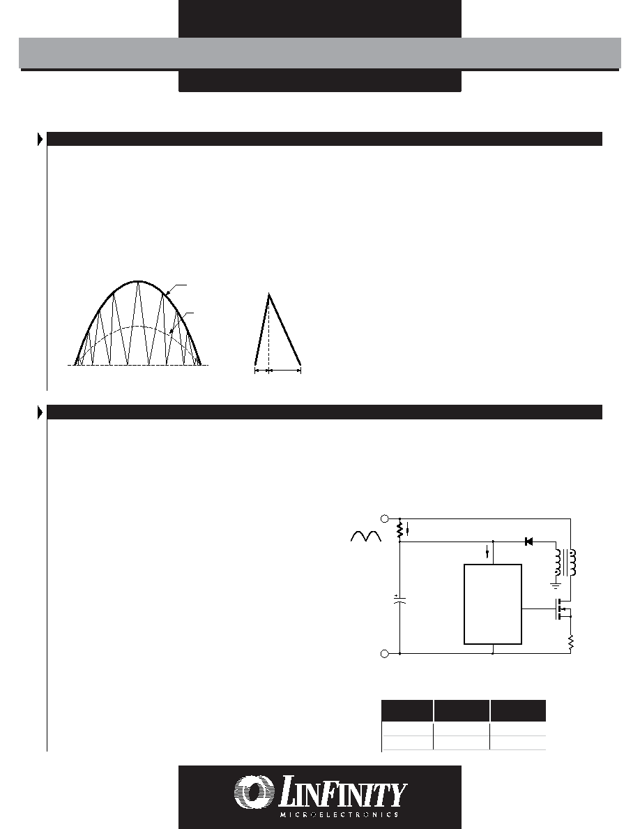
Figure 24 shows an efficient supply voltage using the ultra
low start-up current of the LX1562 in conjunction with a boot-
strap winding off of the power transformer. Circuit operation
is as follows:
The start-up capacitor (C1) is charged by current through
resistor (R1) minus the start-up current drawn by the IC. This
resistor is typically chosen to provide 2X the maximum start-up
current at low line to guarantee start-up under the worst case
condition.
Once the capacitor voltage reaches the start-up
threshold, the IC turns on, starting the switching cycle. The
operation of the IC demands an increase in operating current
which results in discharging the capacitor. During the discharge
cycle, the flyback voltage of the auxiliary winding is rectified
and filtered via rectifier (D1) and charges the capacitor above
the minimum operating voltage of the device and takes over as
the supply voltage. The start-up capacitor and auxiliary wind-
ing must be selected such that it satisfies worst case IC condi-
tions. Figure 25 shows start-up time and voltage of capacitor C1.
Table 1 shows the start-up voltage and hysteresis for LX1562
and LX1563. The LX1562 is used for stand alone pre-regulator
applications while LX1563 is ideal for applications where sup-
ply voltage is derived elsewhere and requires less than 14V
start-up.
Part #
Start-Up
Hysteresis
Voltage
LX1562
13.1V
5.2V
LX1563
9.8V
2.1V
T ABLE 1
Rectified
AC Line
GND
LX1562
GND
V
O
V
IN
I
ST < 300A
I
1 > 300A
C1
R1
R
S
D1
FIGURE 24 — TYPICAL APPLICATION OF START-UP CIRCUITRY
Inductor Peak
Current Envelope
Average
AC Input Current
I
L
T
ON
T
OFF
FIGURE 23 — INDUCTOR CURRENT
O
B
SO
LETE
PRO
D
UCT
NOT
RECOMMENDED
FOR
NEW
DESIGNS
相关PDF资料 |
PDF描述 |
|---|---|
| LX1563IDM-TR | 0.5 A POWER FACTOR CONTROLLER, PDSO8 |
| LX1562IM | 0.5 A POWER FACTOR CONTROLLER, PDIP8 |
| LX1562IDM | 0.5 A POWER FACTOR CONTROLLER, PDSO8 |
| LX1570IDM-TR | 1 A SWITCHING CONTROLLER, PDSO8 |
| LX1571CDM-TR | 1 A SWITCHING CONTROLLER, PDSO8 |
相关代理商/技术参数 |
参数描述 |
|---|---|
| LX1562IM | 功能描述:IC PFC CONTROLLER 8DIP RoHS:是 类别:集成电路 (IC) >> PMIC - PFC(功率因数修正) 系列:- 产品培训模块:GreenChip Synchronous Rectification Control Family of ICs 标准包装:1 系列:- 模式:间歇导电(DCM) 频率 - 开关:- 电流 - 启动:- 电源电压:8.6 V ~ 38 V 工作温度:-20°C ~ 150°C 安装类型:表面贴装 封装/外壳:14-SOIC(0.154",3.90mm 宽) 供应商设备封装:14-SO 包装:Digi-Reel® 其它名称:568-5348-6 |
| LX1563 | 制造商:MICROSEMI 制造商全称:Microsemi Corporation 功能描述:SECOND-GENERATION POWER FACTOR CONTROLLER |
| LX1563IDM | 功能描述:IC CONTROLLER PFC 9.8V 8SOIC RoHS:是 类别:集成电路 (IC) >> PMIC - PFC(功率因数修正) 系列:- 产品培训模块:GreenChip Synchronous Rectification Control Family of ICs 标准包装:1 系列:- 模式:间歇导电(DCM) 频率 - 开关:- 电流 - 启动:- 电源电压:8.6 V ~ 38 V 工作温度:-20°C ~ 150°C 安装类型:表面贴装 封装/外壳:14-SOIC(0.154",3.90mm 宽) 供应商设备封装:14-SO 包装:Digi-Reel® 其它名称:568-5348-6 |
| LX1563IDMT | 制造商:MICROSEMI 制造商全称:Microsemi Corporation 功能描述:Power Factor Controller |
| LX1563IM | 功能描述:IC CONTROLLER PFC 9.8V 8DIP RoHS:是 类别:集成电路 (IC) >> PMIC - PFC(功率因数修正) 系列:- 产品培训模块:GreenChip Synchronous Rectification Control Family of ICs 标准包装:1 系列:- 模式:间歇导电(DCM) 频率 - 开关:- 电流 - 启动:- 电源电压:8.6 V ~ 38 V 工作温度:-20°C ~ 150°C 安装类型:表面贴装 封装/外壳:14-SOIC(0.154",3.90mm 宽) 供应商设备封装:14-SO 包装:Digi-Reel® 其它名称:568-5348-6 |
发布紧急采购,3分钟左右您将得到回复。