- 您现在的位置:买卖IC网 > PDF目录45007 > LX1562IDM-TR (MICROSEMI CORP-ANALOG MIXED SIGNAL GROUP) 0.5 A POWER FACTOR CONTROLLER, PDSO8 PDF资料下载
参数资料
| 型号: | LX1562IDM-TR |
| 厂商: | MICROSEMI CORP-ANALOG MIXED SIGNAL GROUP |
| 元件分类: | 稳压器 |
| 英文描述: | 0.5 A POWER FACTOR CONTROLLER, PDSO8 |
| 封装: | ROHS COMPLIANT, PLASTIC, SOIC-8 |
| 文件页数: | 7/25页 |
| 文件大小: | 430K |
| 代理商: | LX1562IDM-TR |
SECOND-GENERATION POWER FACTOR C ONTROLLER
LX1562/1563
PRODUCT DA T ABOOK 1996/1997
15
Copyright 1996
Rev. 1.3a
8/30
P RODUCTION
D ATA
S HEET
IC DESCRIPTION
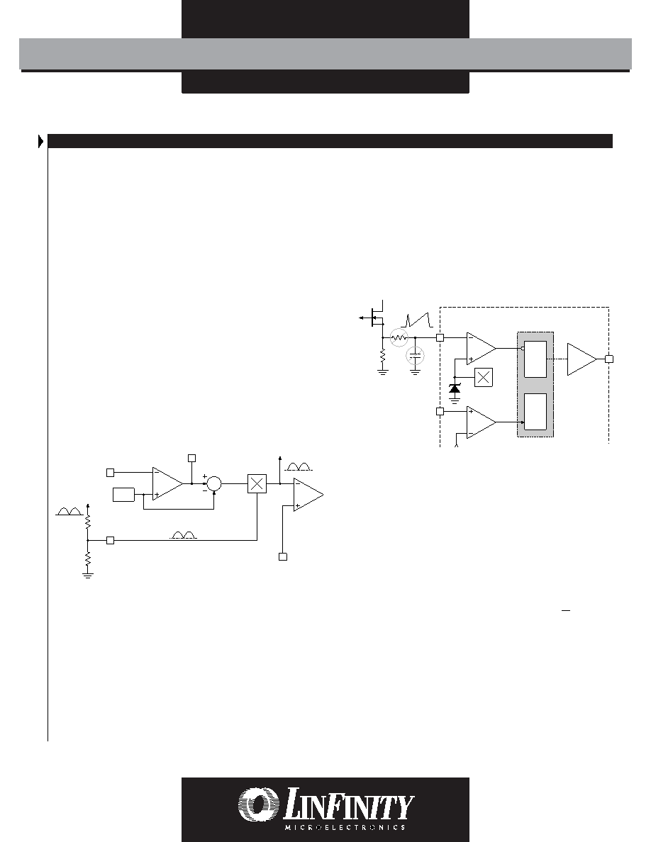
MULTIPLIER
The LX1562/63 features a one quadrant multiplier stage having
two inputs.
One (V
M2) is internally driven by a DC voltage
which is the difference of E.A. output and V
REF. The other (VM1),
is connected to an external resistor divider monitoring the rec-
tified AC line. The output of the multiplier which is a function
of both inputs, controls inductor peak current during each cycle
of operation. This allows the inductor peak current to follow
the AC line thus forcing the average input current to be sinu-
soidal.
The multiplier is in the linear region if the V
M1 input is limited
to less than 2V and the E.A. output is kept below 3.5V under all
line and load conditions. The output is internally clamped to
1.24V typically to limit the MOSFET peak current during turn on
or under excessive load conditions. The equation below de-
scribes the relationship between multiplier output voltage and
the its inputs.
V
M0 = K * VM1 * (V EA0 - VREF)
where:
K = Multiplier gain (typ. 0.65)
V
M1 = Voltage at pin3 (0 to 2V)
V
EA0 = Error amp output voltage (2.5 to 3.5V)
V
M0 = Multiplier output voltage
FIGURE 28 — MULTIPLIER SECTION
for an external RC filter otherwise required for proper opera-
tion of the circuit. This function is described in detail under
“current detect logic” section.
The current sense comparator voltage is limited by an inter-
nal 1.24V (typ.) voltage clamp of the multiplier output. There-
fore maximum switch current is typically given by:
I
PK (MAX) = 1.24V / RS
Maximum switch peak current happens at full load and mini-
mum line conditions.
3
V
AC
R1
R2
Σ
2.5V
V
REF
1
INV.
INPUT
V
M1
V
EA
E.A.
OUTPUT
V
M2
MULT.
OUTPUT
V
M0
4
C.S.
INPUT
2
CURRENT SENSE COMPARATOR
Current sense comparator is configured as a PNP input differ-
ential stage with one input internally tied to the multiplier out-
put and the other available for current sensing. Current is con-
verted to voltage using an external sense resistor in series with
the external power MOSFET. When sense voltage exceeds the
threshold set by the multiplier output, the current sense com-
parator terminates the gate drive to the MOSFET and resets the
PWM latch. The latch insures that the output remains in a low
state after the switch current falls back to zero. The LX1562/63
features a leading edge blanking circuit that eliminates the need
CURRENT DETECT LOGIC
The function of “current detect logic” is to sense the operating
state of the boost inductor and to enable the output driver
accordingly. To achieve this, the downward slope of the in-
ductor current is indirectly detected by monitoring the voltage
across a separate winding and connecting it to the detector
input “I
DET” pin.
Once the inductor current reaches ground
level, the voltage across the winding reverses polarity and
changes the “I
DET” input and the comparator output to the low
state (See Figure 30). When comparator changes state, it sets
the latch and turns on the output driver for a period of 1s
(typ.) regardless of any changes in the latch output (Q) within
this period. This ensures that if the C.S. comparator changes
state due to any turn-on spike, the driver output remains on
and does not turn off prematurely.
However if the spike lasts longer than 1s, the output driver
turns off and the MOSFET stops conducting. This type of digi-
tal current sense blanking which is not amplitude dependent
has higher noise immunity than the commonly used external
RC filtering, allowing for more flexibility in board layout.
Since inductor voltage swings both positive and negative,
internal voltage clamping is provided to protect the IC. The
3
R
S
TO
PIN 7
R
7
1sec
Blank
5
V
M0
Logic
Circuit
FIGURE 29 — CURRENT SENSE SECTION
O
B
SO
LETE
PRO
D
UCT
NOT
RECOMMENDED
FOR
NEW
DESIGNS
相关PDF资料 |
PDF描述 |
|---|---|
| LX1563IDM-TR | 0.5 A POWER FACTOR CONTROLLER, PDSO8 |
| LX1562IM | 0.5 A POWER FACTOR CONTROLLER, PDIP8 |
| LX1562IDM | 0.5 A POWER FACTOR CONTROLLER, PDSO8 |
| LX1570IDM-TR | 1 A SWITCHING CONTROLLER, PDSO8 |
| LX1571CDM-TR | 1 A SWITCHING CONTROLLER, PDSO8 |
相关代理商/技术参数 |
参数描述 |
|---|---|
| LX1562IM | 功能描述:IC PFC CONTROLLER 8DIP RoHS:是 类别:集成电路 (IC) >> PMIC - PFC(功率因数修正) 系列:- 产品培训模块:GreenChip Synchronous Rectification Control Family of ICs 标准包装:1 系列:- 模式:间歇导电(DCM) 频率 - 开关:- 电流 - 启动:- 电源电压:8.6 V ~ 38 V 工作温度:-20°C ~ 150°C 安装类型:表面贴装 封装/外壳:14-SOIC(0.154",3.90mm 宽) 供应商设备封装:14-SO 包装:Digi-Reel® 其它名称:568-5348-6 |
| LX1563 | 制造商:MICROSEMI 制造商全称:Microsemi Corporation 功能描述:SECOND-GENERATION POWER FACTOR CONTROLLER |
| LX1563IDM | 功能描述:IC CONTROLLER PFC 9.8V 8SOIC RoHS:是 类别:集成电路 (IC) >> PMIC - PFC(功率因数修正) 系列:- 产品培训模块:GreenChip Synchronous Rectification Control Family of ICs 标准包装:1 系列:- 模式:间歇导电(DCM) 频率 - 开关:- 电流 - 启动:- 电源电压:8.6 V ~ 38 V 工作温度:-20°C ~ 150°C 安装类型:表面贴装 封装/外壳:14-SOIC(0.154",3.90mm 宽) 供应商设备封装:14-SO 包装:Digi-Reel® 其它名称:568-5348-6 |
| LX1563IDMT | 制造商:MICROSEMI 制造商全称:Microsemi Corporation 功能描述:Power Factor Controller |
| LX1563IM | 功能描述:IC CONTROLLER PFC 9.8V 8DIP RoHS:是 类别:集成电路 (IC) >> PMIC - PFC(功率因数修正) 系列:- 产品培训模块:GreenChip Synchronous Rectification Control Family of ICs 标准包装:1 系列:- 模式:间歇导电(DCM) 频率 - 开关:- 电流 - 启动:- 电源电压:8.6 V ~ 38 V 工作温度:-20°C ~ 150°C 安装类型:表面贴装 封装/外壳:14-SOIC(0.154",3.90mm 宽) 供应商设备封装:14-SO 包装:Digi-Reel® 其它名称:568-5348-6 |
发布紧急采购,3分钟左右您将得到回复。