- 您现在的位置:买卖IC网 > PDF目录180125 > M28W800BB100ZB1 (STMICROELECTRONICS) 512K X 16 FLASH 3V PROM, 100 ns, PBGA46 PDF资料下载
参数资料
| 型号: | M28W800BB100ZB1 |
| 厂商: | STMICROELECTRONICS |
| 元件分类: | PROM |
| 英文描述: | 512K X 16 FLASH 3V PROM, 100 ns, PBGA46 |
| 封装: | 6.39 X 6.37 MM, 0.75 MM PITCH, TFBGA-46 |
| 文件页数: | 38/42页 |
| 文件大小: | 289K |
| 代理商: | M28W800BB100ZB1 |
第1页第2页第3页第4页第5页第6页第7页第8页第9页第10页第11页第12页第13页第14页第15页第16页第17页第18页第19页第20页第21页第22页第23页第24页第25页第26页第27页第28页第29页第30页第31页第32页第33页第34页第35页第36页第37页当前第38页第39页第40页第41页第42页
5/42
M28W800BT, M28W800BB
SUMMARY DESCRIPTION
The M28W800B is a 8 Mbit (512Kbit x 16) non-vol-
atileFlash memory that canbeerasedelectrically
at the block level and programmed in-system on a
Word-by-Word basis. These operations can be
performed using a single low voltage (2.7 to 3.6V)
supply. VDDQ allows to drive the I/O pin down to
1.65V. An optional 12V VPP power supply is pro-
vided to speed up customer programming.
The device features an asymmetrical blocked ar-
chitecture. The M28W800B has an array of 23
blocks: 8 Parameter Blocks of 4 KWord and 15
Main Blocks of 32 KWord. M28W800BT has the
Parameter Blocks at the top of the memory ad-
dress space while the M28W800BB locates the
Parameter Blocks starting from the bottom. The
memory maps are shown in Figure 5, Block Ad-
dresses.
Parameter blocks 0 and 1 can be protected from
accidental programming or erasure. Each block
can be erased separately. Erase can be suspend-
ed in order to perform either read or program in
any other block and then resumed. Program can
be suspended to read data in any other block and
then resumed. Each block can be programmed
and erased over 100,000 cycles.
Program and Erase commands are written to the
Command Interface of the memory. An on-chip
Program/Erase Controller takes care of the tim-
ings necessary for program and erase operations.
The end of a program or erase operation can be
detected and any error conditions identified. The
command set required to control the memory is
consistent with JEDEC standards.
The memory is offered in TSOP48 (10 X 20mm),
and TFBGA46 (6.39 x 6.37mm, 0.75mm pitch)
packages and is supplied with all the bits erased
(set to ’1’).
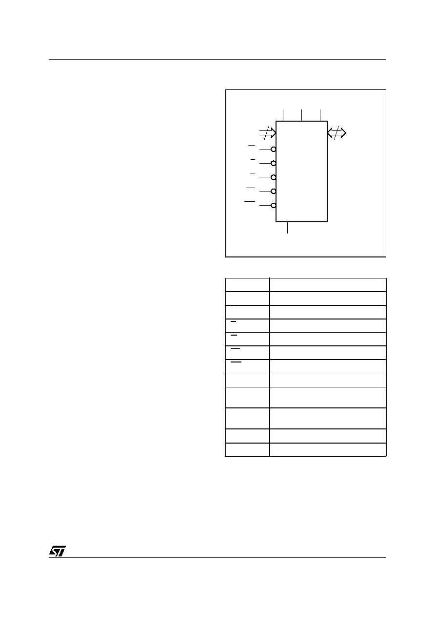
Figure 2. Logic Diagram
Table 1. Signal Names
A0-A18
Address Inputs
DQ0-DQ15
Data Input/Output
E
Chip Enable
G
Output Enable
W
Write Enable
RP
Reset
WP
Write Protect
VDD
Core Power Supply
VDDQ
Power Supply for
Input/Output
VPP
Optional Supply Voltage for
Fast Program & Erase
VSS
Ground
NC
Not Connected Internally
AI03581
19
A0-A18
W
DQ0-DQ15
VDD
M28W800BT
M28W800BB
E
VSS
16
G
RP
WP
VDDQ VPP
相关PDF资料 |
PDF描述 |
|---|---|
| M29F102B-90N1TR | 64K X 16 FLASH 5V PROM, 90 ns, PDSO40 |
| M29F200BB70MT3 | 128K X 16 FLASH 5V PROM, 70 ns, PDSO44 |
| M29F400BT45M1E | 256K X 16 FLASH 5V PROM, 45 ns, PDSO44 |
| M29F400FB55M3F2 | 256K X 16 FLASH 5V PROM, 55 ns, PDSO44 |
| M29F400FB5AN6F2 | 256K X 16 FLASH 5V PROM, 55 ns, PDSO48 |
相关代理商/技术参数 |
参数描述 |
|---|---|
| M28W800BB90N1 | 功能描述:闪存 8M (512Kx16) 70ns RoHS:否 制造商:ON Semiconductor 数据总线宽度:1 bit 存储类型:Flash 存储容量:2 MB 结构:256 K x 8 定时类型: 接口类型:SPI 访问时间: 电源电压-最大:3.6 V 电源电压-最小:2.3 V 最大工作电流:15 mA 工作温度:- 40 C to + 85 C 安装风格:SMD/SMT 封装 / 箱体: 封装:Reel |
| M28W800BB90ZB6T | 功能描述:闪存 8M (512Kx16) 90ns RoHS:否 制造商:ON Semiconductor 数据总线宽度:1 bit 存储类型:Flash 存储容量:2 MB 结构:256 K x 8 定时类型: 接口类型:SPI 访问时间: 电源电压-最大:3.6 V 电源电压-最小:2.3 V 最大工作电流:15 mA 工作温度:- 40 C to + 85 C 安装风格:SMD/SMT 封装 / 箱体: 封装:Reel |
| M28W800BT100N6T | 功能描述:闪存 8M (512Kx16) 100ns RoHS:否 制造商:ON Semiconductor 数据总线宽度:1 bit 存储类型:Flash 存储容量:2 MB 结构:256 K x 8 定时类型: 接口类型:SPI 访问时间: 电源电压-最大:3.6 V 电源电压-最小:2.3 V 最大工作电流:15 mA 工作温度:- 40 C to + 85 C 安装风格:SMD/SMT 封装 / 箱体: 封装:Reel |
| M28W800BT90N6 | 制造商:Micron Technology Inc 功能描述:FLASH PARALLEL 3V/3.3V 8MBIT 512KX16 90NS 48TSOP - Trays |
| M28W800CB90N1 | 功能描述:闪存 8M (512Kx16) 90ns RoHS:否 制造商:ON Semiconductor 数据总线宽度:1 bit 存储类型:Flash 存储容量:2 MB 结构:256 K x 8 定时类型: 接口类型:SPI 访问时间: 电源电压-最大:3.6 V 电源电压-最小:2.3 V 最大工作电流:15 mA 工作温度:- 40 C to + 85 C 安装风格:SMD/SMT 封装 / 箱体: 封装:Reel |
发布紧急采购,3分钟左右您将得到回复。