- 您现在的位置:买卖IC网 > PDF目录45016 > M30600E8GP 16-BIT, OTPROM, 10 MHz, MICROCONTROLLER, PQFP100 PDF资料下载
参数资料
| 型号: | M30600E8GP |
| 元件分类: | 微控制器/微处理器 |
| 英文描述: | 16-BIT, OTPROM, 10 MHz, MICROCONTROLLER, PQFP100 |
| 封装: | 14 X 14 MM, 0.50 MM PITCH, PLASTIC, LQFP-100 |
| 文件页数: | 57/139页 |
| 文件大小: | 1782K |
| 代理商: | M30600E8GP |
第1页第2页第3页第4页第5页第6页第7页第8页第9页第10页第11页第12页第13页第14页第15页第16页第17页第18页第19页第20页第21页第22页第23页第24页第25页第26页第27页第28页第29页第30页第31页第32页第33页第34页第35页第36页第37页第38页第39页第40页第41页第42页第43页第44页第45页第46页第47页第48页第49页第50页第51页第52页第53页第54页第55页第56页当前第57页第58页第59页第60页第61页第62页第63页第64页第65页第66页第67页第68页第69页第70页第71页第72页第73页第74页第75页第76页第77页第78页第79页第80页第81页第82页第83页第84页第85页第86页第87页第88页第89页第90页第91页第92页第93页第94页第95页第96页第97页第98页第99页第100页第101页第102页第103页第104页第105页第106页第107页第108页第109页第110页第111页第112页第113页第114页第115页第116页第117页第118页第119页第120页第121页第122页第123页第124页第125页第126页第127页第128页第129页第130页第131页第132页第133页第134页第135页第136页第137页第138页第139页
Mitsubishi microcomputers
M16C / 60 Group
SINGLE-CHIP 16-BIT CMOS MICROCOMPUTER
24
Bus Control
The following explains the signals required for accessing external devices and software waits. The signals
required for accessing the external devices are valid when the processor mode is set to memory expansion
mode and microprocessor mode. The software waits are valid in all processor modes.
(1) Address bus/data bus
The address bus consists of the 20 pins A0 to A19 for accessing the 1M bytes of address space.
The data bus consists of the pins for data I/O. When the BYTE pin is “H”, the 8 ports D0 to D7 function
as the data bus. When BYTE is “L”, the 16 ports D0 to D15 function as the data bus.
Both the address and data bus retain their previous states when internal ROM or RAM is accessed.
Also, when a change is made from single-chip mode to memory expansion mode, the value of the
address bus is undefined until external memory is accessed.
(2) Chip select signal
The chip select signal is output using the same pins as P44 to P47. Bits 0 to 3 of the chip select control
register (address 000816) set each pin to function as a port or to output the chip select signal. The chip
select control register is valid in memory expansion mode and microprocessor mode. In single-chip
mode, P44 to P47 function as programmable I/O ports regardless of the value in the chip select control
register.
_______
In microprocessor mode, only CS0 outputs the chip select signal after the reset state has been can-
_______
celled. CS1 to CS3 function as input ports. Therefore, when using CS1 to CS3, external pull-up resis-
tors are required. Figure 1.16 shows the configuration of the chip select control register.
The chip select signal can be used to split the external area into as many as four blocks. Table 1.6
shows the external memory areas specified using the chip select signal.
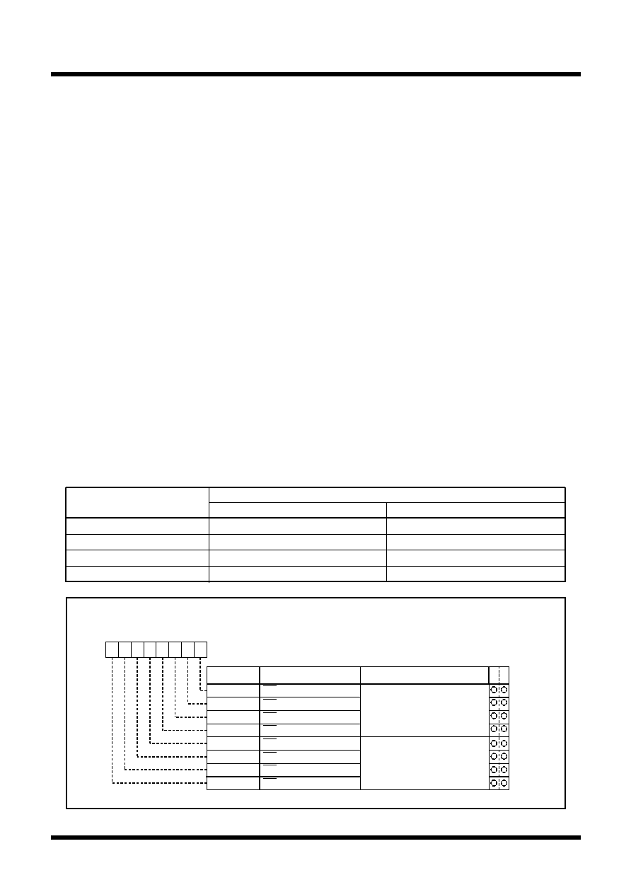
Figure 1.16. Configuration of chip select control register
Chip select control register
Symbol
Address
When reset
CSR
0008 16
01 16
Bit name
Function
W
R
b7
b6
b5
b4
b3
b2
b1
b0
CS1 output enable bit
CS1
CS0
CS3
CS2
CS0 output enable bit
CS2 output enable bit
CS3 output enable bit
CS1W
CS0W
CS3W
CS2W
CS0 wait bit
CS1 wait bit
CS2 wait bit
CS3 wait bit
0 : Chip select output disabled
(Normal port pin)
1 : Chip select output enabled
0 : Wait state inserted
1 : No wait state
Bit symbol
Bus Control
Chip select
Specified address range
Memory expansion mode
Microprocessor mode
_______
CS0
9000016 to CFFFF16(256K)
9000016 to FFFFF16
(448K)
_______
CS1
1000016 to 8FFFF16(512K)
1000016 to 8FFFF16
(512K)
_______
CS2
0800016 to 0FFFF16 (32K)
0800016 to 0FFFF16
(32K)
_______
CS3
0400016 to 07FFF16 (16K)
0400016 to 07FFF16
(16K)
Table 1.6. External areas specified by the chip select signals
相关PDF资料 |
PDF描述 |
|---|---|
| M30600M8-XXXGP | 16-BIT, MROM, MICROCONTROLLER, PQFP100 |
| M30610MCA-XXXGP | 16-BIT, MROM, 10 MHz, MICROCONTROLLER, PQFP100 |
| M30610ECFS | 16-BIT, UVPROM, 10 MHz, MICROCONTROLLER, CQCC100 |
| M30612M4A-XXXGP | 16-BIT, MROM, 10 MHz, MICROCONTROLLER, PQFP100 |
| M30610ECGP | 16-BIT, OTPROM, 10 MHz, MICROCONTROLLER, PQFP100 |
相关代理商/技术参数 |
参数描述 |
|---|---|
| M30-6011046 | 制造商:Harwin 功能描述: |
| M30-6011506 | 功能描述:集管和线壳 15 + 15 DIL SMT PLUG RoHS:否 产品种类:1.0MM Rectangular Connectors 产品类型:Headers - Pin Strip 系列:DF50 触点类型:Pin (Male) 节距:1 mm 位置/触点数量:16 排数:1 安装风格:SMD/SMT 安装角:Right 端接类型:Solder 外壳材料:Liquid Crystal Polymer (LCP) 触点材料:Brass 触点电镀:Gold 制造商:Hirose Connector |
| M30-6011546 | 功能描述:集管和线壳 30P Male Dual Row Vertical SMT RoHS:否 产品种类:1.0MM Rectangular Connectors 产品类型:Headers - Pin Strip 系列:DF50 触点类型:Pin (Male) 节距:1 mm 位置/触点数量:16 排数:1 安装风格:SMD/SMT 安装角:Right 端接类型:Solder 外壳材料:Liquid Crystal Polymer (LCP) 触点材料:Brass 触点电镀:Gold 制造商:Hirose Connector |
| M30-6012046 | 制造商:Harwin 功能描述: |
| M3060C | 制造商:VISHAY 制造商全称:Vishay Siliconix 功能描述:Dual Common-Cathode Schottky Rectifier |
发布紧急采购,3分钟左右您将得到回复。