- 您现在的位置:买卖IC网 > PDF目录69009 > M306N5FCTGP 16-BIT, FLASH, 20 MHz, MICROCONTROLLER, PQFP100 PDF资料下载
参数资料
| 型号: | M306N5FCTGP |
| 元件分类: | 微控制器/微处理器 |
| 英文描述: | 16-BIT, FLASH, 20 MHz, MICROCONTROLLER, PQFP100 |
| 封装: | 14 X 14 MM, 0.50 MM PITCH, PLASTIC, LQFP-100 |
| 文件页数: | 58/63页 |
| 文件大小: | 825K |
| 代理商: | M306N5FCTGP |
第1页第2页第3页第4页第5页第6页第7页第8页第9页第10页第11页第12页第13页第14页第15页第16页第17页第18页第19页第20页第21页第22页第23页第24页第25页第26页第27页第28页第29页第30页第31页第32页第33页第34页第35页第36页第37页第38页第39页第40页第41页第42页第43页第44页第45页第46页第47页第48页第49页第50页第51页第52页第53页第54页第55页第56页第57页当前第58页第59页第60页第61页第62页第63页
Serial I/O
Mitsubishi microcomputers
M16C / 62A Group (80-pin)
SINGLE-CHIP 16-BIT CMOS MICROCOMPUTER
86
Serial I/O
Serial I/O is configured as five channels: UART0, UART1, UART2, S I/O3 and S I/O4.
UART0 to 2
UART0, UART1 and UART2 each have an exclusive timer to generate a transfer clock, so they operate
independently of each other.
Figure 1.14.1 shows the block diagram of UART0, UART1 and UART2. Figures 1.14.2 and 1.14.3 show
the block diagram of the transmit/receive unit.
UARTi (i = 0 to 2) has two operation modes: a clock synchronous serial I/O mode and a clock asynchronous
serial I/O mode (UART mode). The contents of the serial I/O mode select bits (bits 0 to 2 at addresses
03A016, 03A816 and 037816) determine whether UARTi is used as a clock synchronous serial I/O or as a
UART.
UART0 through UART2 are almost equal in their functions with minor exceptions. UART2, in particular, is
used for the SIM interface with some extra settings added in clock-asynchronous serial I/O mode (Note). It
also has the bus collision detection function that generates an interrupt request if the TxD pin and the RxD
pin are different in level. UART and IIC mode can be used in UART2.
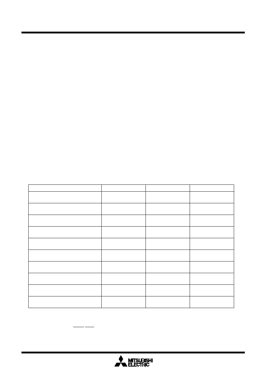
Table 1.14.1 shows the comparison of functions of UART0 through UART2, and Figures 1.14.4 to 1.14.9
show the registers related to UARTi.
Note: SIM : Subscriber Identity Module
UART0
UART1
UART2
Function
CLK polarity selection
Continuous receive mode selection
LSB first / MSB first selection
Impossible
Transfer clock output from multiple
pins selection
Impossible
Serial data logic switch
Impossible
Sleep mode selection
Impossible
TxD, RxD I/O polarity switch
Impossible
Possible
CMOS output
TxD, RxD port output format
CMOS output
N-channel open-drain
output
Impossible
Parity error signal output
Impossible
Bus collision detection
Impossible
Possible
(Note 1)
Possible
(Note 1)
Possible
(Note 1)
Possible
(Note 3)
Possible
(Note 1)
Possible
(Note 1)
Possible
(Note 1)
Possible
(Note 1)
Possible
(Note 3)
Possible
(Note 5)
Possible
(Note 2)
Possible
(Note 1)
Possible
(Note 4)
Possible
(Note 4)
(Note 5)
(Note 6)
Note 1: Only when clock synchronous serial I/O mode.
Note 2: Only when clock synchronous serial I/O mode and 8-bit UART mode.
Note 3: Only when UART mode.
Note 4: Using for SIM interface.
Note 5: Since CLK2 and CTS2/RTS2 do not connect to outside, this function cannot be used.
Note 6: Connect this pin to Vcc via a pull-up resistor on the outside.
Table 1.14.1. Comparison of functions of UART0 through UART2
相关PDF资料 |
PDF描述 |
|---|---|
| M306N5FCFP | 16-BIT, FLASH, 24 MHz, MICROCONTROLLER, PQFP100 |
| M306N5FCVFP | 16-BIT, FLASH, 20 MHz, MICROCONTROLLER, PQFP100 |
| M306N5FCVGP | 16-BIT, FLASH, 20 MHz, MICROCONTROLLER, PQFP100 |
| M306N5MCT-XXXGP | 16-BIT, MROM, 20 MHz, MICROCONTROLLER, PQFP100 |
| M306V0ME-XXXFP | 16-BIT, MROM, MICROCONTROLLER, PQFP100 |
相关代理商/技术参数 |
参数描述 |
|---|---|
| M306N5FCVFP | 制造商:RENESAS 制造商全称:Renesas Technology Corp 功能描述:Renesas MCU |
| M306N5FCVGP | 制造商:RENESAS 制造商全称:Renesas Technology Corp 功能描述:Renesas MCU |
| M306N5MCT-XXXFP | 制造商:RENESAS 制造商全称:Renesas Technology Corp 功能描述:Renesas MCU |
| M306N5MCT-XXXGP | 制造商:RENESAS 制造商全称:Renesas Technology Corp 功能描述:Renesas MCU |
| M306N5MCV-XXXFP | 制造商:RENESAS 制造商全称:Renesas Technology Corp 功能描述:Renesas MCU |
发布紧急采购,3分钟左右您将得到回复。