- 您现在的位置:买卖IC网 > PDF目录67761 > M32000D4BFP-80 32-BIT, 80 MHz, MICROCONTROLLER, PQFP100 PDF资料下载
参数资料
| 型号: | M32000D4BFP-80 |
| 元件分类: | 微控制器/微处理器 |
| 英文描述: | 32-BIT, 80 MHz, MICROCONTROLLER, PQFP100 |
| 封装: | 14 X 20 MM, 0.65 MM PITCH, PLASTIC, LQFP-100 |
| 文件页数: | 17/44页 |
| 文件大小: | 448K |
| 代理商: | M32000D4BFP-80 |
第1页第2页第3页第4页第5页第6页第7页第8页第9页第10页第11页第12页第13页第14页第15页第16页当前第17页第18页第19页第20页第21页第22页第23页第24页第25页第26页第27页第28页第29页第30页第31页第32页第33页第34页第35页第36页第37页第38页第39页第40页第41页第42页第43页第44页
SINGLE-CHIP 32-BIT CMOS MICROCOMPUTER
MITSUBISHI MICROCOMPUTERS
M32000D4BFP-80
24
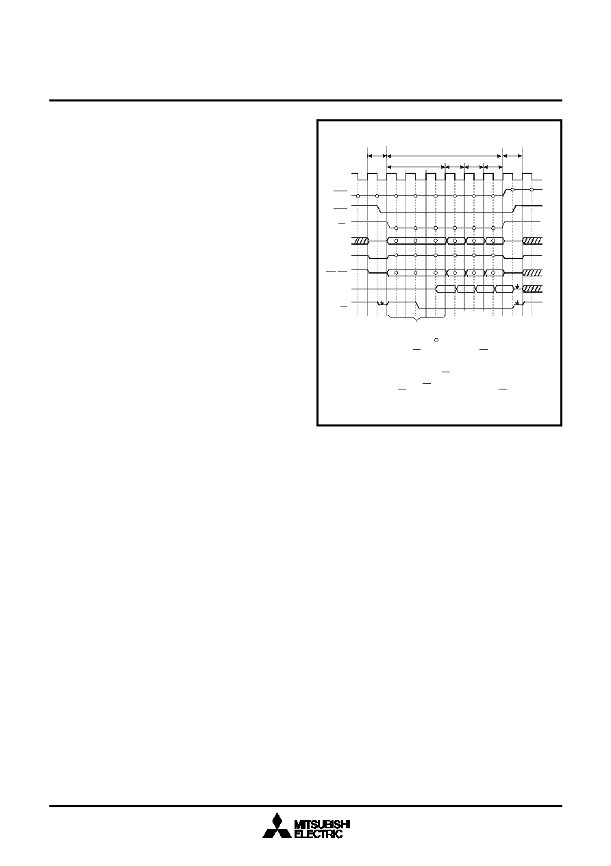
When the M32000D4BFP-80 is in the hold state and an "L" level is
__
input to CS, the M32000D4BFP-80 interprets it as a bus access re-
__
quest to the internal DRAM. In this case, when the R/W signal is an
"H" level, the memory controller drives a read cycle to the internal
DRAM. In the read cycle, the 16-bit data for the address specified
____
with A8 to A30, is output from D0 to D15 regardless of the BCH and
___
__
BCL settings. Also the DC signal is output.
The M32000D4BFP-80 reads 128 bits of data from the block on the
128-bit boundary including the requested address into the 128-bit
buffer of the bus interface unit. 3 to 7 CLKIN clock periods are neces-
sary for the first bus access, however, when reading consecutive
address within the 128-bit boundary, the subsequent read bus cycles
are completed in 1 CLKIN clock period because a read from the in-
ternal DRAM does not take place.
Once the external bus master read cycle has been driven, it cannot
__
be aborted. When an "L" level is input to CS and an access has
started, the values of this and other control signals should be held
__
during the wait cycles (that is while DC = "H"). After DC outputs an
__
"L" level (access complete), return CS to the "H" level between the
CLKIN falling edge corresponding to the last read cycle and the fol-
______
lowing CLKIN falling edge. Return HREQ to the "H" level to return
the M32000D4BFP-80 to the normal operation mode from the hold
__
state either at the same time as or after CS is returned to the "H"
level.
Fig. 23 Read bus cycle to internal DRAM
("L" output)
"Hi-Z"
V
HREQ
BCH, BCL
D0 - D15
DC
R/W
hold shift
hold
return
HACK
A8 - A30
CS
read
Note: "Hi-Z" means high impedance, and
indicates sampling timing.
CLKIN
The value of the R/W signal that controls the data direction of the bus interface
cannot be changed during CS="L". Hold this value while CS="L".
Also, where marked above with V, 3 to 7 CLKIN clock periods are necessary for
the first read operation (also when reading crosses an 128-bit boundary) when
reading from the internal DRAM. Hold the input value of the address or other control
signals during these wait cycle periods (DC = "H"). Consecutive read operations
within an 128-bit boundary are completed in 1 CLKIN clock period.
During these wait cycle period, CS cannot be returned to an "H" level (the access
cannot be aborted). CS can only be returned to an "H" level after DC is driven to "L".
相关PDF资料 |
PDF描述 |
|---|---|
| M32171F4VFP | 32-BIT, MROM, 40 MHz, MICROCONTROLLER, PQFP144 |
| M32171F3VFP | 32-BIT, MROM, 40 MHz, MICROCONTROLLER, PQFP144 |
| M32173F2VFP | 32-BIT, FLASH, 40 MHz, RISC MICROCONTROLLER, PQFP144 |
| M32172F2VFP | 32-BIT, FLASH, 40 MHz, RISC MICROCONTROLLER, PQFP144 |
| M32186F8VFP | 32-BIT, FLASH, 80 MHz, RISC MICROCONTROLLER, PQFP144 |
相关代理商/技术参数 |
参数描述 |
|---|---|
| M32002AGLJ | 制造商:MTRONPTI 制造商全称:MTRONPTI 功能描述:9x14 mm, 3.3/2.5/1.8 Volt, PECL/LVDS/CML, VCXO |
| M32002AGMJ | 制造商:MTRONPTI 制造商全称:MTRONPTI 功能描述:9x14 mm, 3.3/2.5/1.8 Volt, PECL/LVDS/CML, VCXO |
| M32002AGPJ | 制造商:MTRONPTI 制造商全称:MTRONPTI 功能描述:9x14 mm, 3.3/2.5/1.8 Volt, PECL/LVDS/CML, VCXO |
| M32002AMLJ | 制造商:MTRONPTI 制造商全称:MTRONPTI 功能描述:9x14 mm, 3.3/2.5/1.8 Volt, PECL/LVDS/CML, VCXO |
| M32002AMMJ | 制造商:MTRONPTI 制造商全称:MTRONPTI 功能描述:9x14 mm, 3.3/2.5/1.8 Volt, PECL/LVDS/CML, VCXO |
发布紧急采购,3分钟左右您将得到回复。