- 您现在的位置:买卖IC网 > PDF目录69010 > M34238MK-XXXGP 4-BIT, MROM, 4 MHz, MICROCONTROLLER, PDSO20 PDF资料下载
参数资料
| 型号: | M34238MK-XXXGP |
| 元件分类: | 微控制器/微处理器 |
| 英文描述: | 4-BIT, MROM, 4 MHz, MICROCONTROLLER, PDSO20 |
| 封装: | PLASTIC, SOP-20 |
| 文件页数: | 40/41页 |
| 文件大小: | 243K |
| 代理商: | M34238MK-XXXGP |
第1页第2页第3页第4页第5页第6页第7页第8页第9页第10页第11页第12页第13页第14页第15页第16页第17页第18页第19页第20页第21页第22页第23页第24页第25页第26页第27页第28页第29页第30页第31页第32页第33页第34页第35页第36页第37页第38页第39页当前第40页第41页
MITSUBISHI MICROCOMPUTERS
4238 Group
SINGLE-CHIP 4-BIT CMOS MICROCOMPUTER for INFRARED REMOTE CONTROL TRANSMITTERS
7
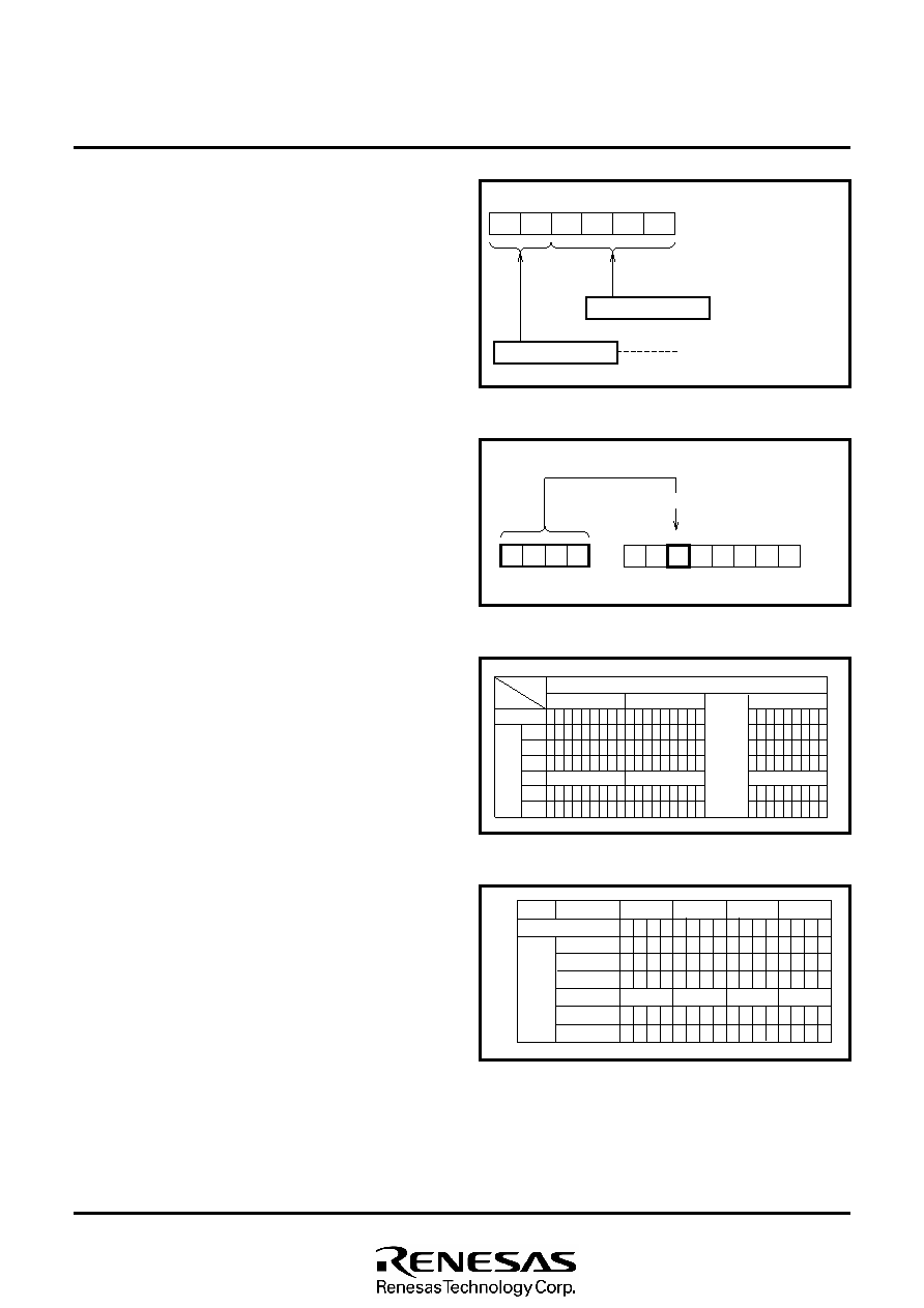
DATA POINTER (DP)
Data pointer (DP) is used to specify a RAM address and consists of
registers X and Y. Register X specifies a file, and register Y specifies
a RAM digit.
Register Y is also used to specify the port D bit position.
When port D is used, set the port D bit position to register Y and its
output latch is set with the SD instruction or is cleared with the RD
instruction, and then, select its I/O function.
PROGRAM MEMORY (ROM)
The program memory is a mask ROM and stores the instruction
codes. ROM size is 768 words
× 9 bits. ROM is separated every 128
words (addresses 0 to 127) by the unit of page (6 pages). Figure 10
shows the ROM address map.
Page 2 is the special page for subroutine calls. Subroutines written in
this page can be called from any page with the 1-word instruction
(BM). Subroutines extending from page 2 to another page can also
be called with the BM instruction when it starts on page 2.
All pages can be used as data areas with the TABP p instruction (p=0
to 5). However, 1 stage of stack is used when the TABP p instruction
is executed.
DATA MEMORY (RAM)
Data memory (RAM) stores processing data and control data. RAM
size is 32 words
× 4 bits (128 bits). 1 word of RAM is composed of 4
bits, but 1-bit manipulation (with the SB j, RB j, and SZB j instruc-
tions) is enabled for the entire memory area. A RAM address is
specified by a data pointer. The data pointer consists of registers X
and Y. Set a value to the data pointer certainly when executing an
instruction to access RAM. Figure 11 shows the RAM address map.
Fig. 8 Data pointer (DP) structure
Fig. 9 SD instruction execution example
Fig. 10 ROM address map
Fig. 11 RAM address map
01
1
D7
D5
D0
Specifying bit position
Register Y (4)
Port D output latch
Set
X1
X0
Y3
Y2
Y1
Y0
Data pointer DP
Register Y (4)
Specifying RAM file
Specifying RAM digit
Register X (2)
32
0
1 032 1
1
0
1
2
…
6
7
File
Register X
Bit
Digit
(Register
Y)
32 1
2
0
…
32 1
3
0
…
8765 4 3 210 8765 4 3 210
8765 4 3 210
0
1
2
126
127
…
PCL
PCH
Page
Address
Bit
01
.....
5
相关PDF资料 |
PDF描述 |
|---|---|
| M34250E2-XXXFP | 4-BIT, OTPROM, 4.4 MHz, MICROCONTROLLER, PDSO20 |
| M34250M2-XXXFP | 4-BIT, MROM, 4.4 MHz, MICROCONTROLLER, PDSO20 |
| M34250M2-XXXFP | 4-BIT, MROM, 4.4 MHz, MICROCONTROLLER, PDSO20 |
| M34280M1-XXXFP | 4-BIT, MROM, 4 MHz, MICROCONTROLLER, PDSO20 |
| M34280M1-XXXGP | 4-BIT, MROM, 4 MHz, MICROCONTROLLER, PDSO20 |
相关代理商/技术参数 |
参数描述 |
|---|---|
| M3424 SL001 | 制造商:Alpha Wire Company 功能描述:CBL 6PR 24AWG SLT 1000' |
| M3424 SL002 | 制造商:Alpha Wire Company 功能描述:CBL 6PR 24AWG SLT 500' |
| M3424 SL005 | 制造商:Alpha Wire Company 功能描述:CBL 6PR 24AWG SLT 100' |
| M3424-0003 | 制造商:Bonitron 功能描述:OVERVOLTAGE BRAKING TRANSISTOR |
| M3424-SL002 | 制造商:Alpha Wire 功能描述: |
发布紧急采购,3分钟左右您将得到回复。