- 您现在的位置:买卖IC网 > PDF目录69010 > M34238MK-XXXGP 4-BIT, MROM, 4 MHz, MICROCONTROLLER, PDSO20 PDF资料下载
参数资料
| 型号: | M34238MK-XXXGP |
| 元件分类: | 微控制器/微处理器 |
| 英文描述: | 4-BIT, MROM, 4 MHz, MICROCONTROLLER, PDSO20 |
| 封装: | PLASTIC, SOP-20 |
| 文件页数: | 8/41页 |
| 文件大小: | 243K |
| 代理商: | M34238MK-XXXGP |
第1页第2页第3页第4页第5页第6页第7页当前第8页第9页第10页第11页第12页第13页第14页第15页第16页第17页第18页第19页第20页第21页第22页第23页第24页第25页第26页第27页第28页第29页第30页第31页第32页第33页第34页第35页第36页第37页第38页第39页第40页第41页
MITSUBISHI MICROCOMPUTERS
4238 Group
SINGLE-CHIP 4-BIT CMOS MICROCOMPUTER for INFRARED REMOTE CONTROL TRANSMITTERS
15
PRECAUTION FOR USE
1
Notes on noise and latch-up
In order to avoid noise and latch-up, connect a bypass capacitor
(
≈0.1
F) directly between the VDD pin and VSS pin using the thickest
possible wire, and equalize its wiring in width and length.
2
Notes on instruction clock switch function
Note the following about the instruction clock switch function;
1. The CCK instruction can be used only at address 0 in page 0.
2. Note that the selective range of system clock signal f(XIN) varies
depending on whether to use the CCK instruction as shown in
Table 2.
CCK instruction
Used
Not used
Table 2 Selective range of f(XIN) frequency
3
Note on external clock
When using an external clock, do not stop the clock except at the
RAM back-up state.
When using an external clock, its duty ratio must be 30 to 70%.
4
Notes on internal state when system is released from reset, or
is returned from the RAM back-up state or standby state
Figure 19 shows the internal state when system is released from re-
set, or is returned from the RAM back-up state or standby state. In
the RAM back-up state, data except RAM is not retained and is ini-
tialized as shown in Figure 19.
Instruction clock
f(XIN)/4
f(XIN)/32
f(XIN) frequency
300 kHz to 500 kHz
2.4 MHz to 4.0 MHz
Program counter (PC) .............
(address 0 in page 0 is set to PC)
Machine cycle count value select register MC .......................
Carrier wave select register C ......................................
Logic operation select register LO ...............................
Port output latch (D, E, CARR) ....................................
Port output latch (G) ................................................
Registers A and B ..................................................
Power down flag (P)
When system is released from reset, and is returned from
standby state ..........................................................................
When system is returned from RAM back-up state ...............
Registers and flags other than above are undefined when system is re-
leased from reset, and is returned from the RAM back-up state and
standby state. Set initial values when system is released from reset,
and is returned from the RAM back-up state and standby state.
5
Setting of unused pins
Set the unused pins as shown in Table 3.
Table 3. Setting of unused pins
Setting
Open
Set the port D output latches to “0” and open, or
connect to VSS (Note).
Open
Pin
XOUT
RESET
D0 – D7
E, G0 – G3
(Note when the output latch is set to “0” and pins are open)
Port D output latches are set to “1” when system is released from
reset, or is returned from the RAM back-up state or standby state.
Clear the port D output latches to “0” by software.
The voltage of pins is undefined until the port D output latches are
set to “0”, and the supply current may be increased.
To set the output latch periodically by software is recommended
because value of output latch may change by noise or program
run-away (caused by noise).
(Note when connecting to VSS)
Connect the unused pins to VSS at the shortest distance (within
2cm) using the thickest possible wire in order to prevent noise.
6
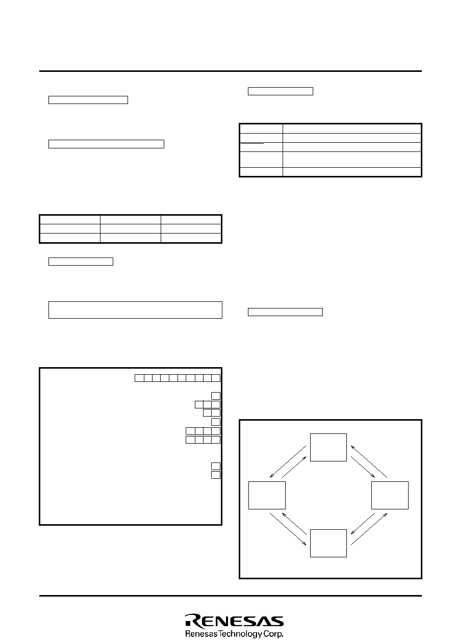
Notes on the stack pointer
Stack pointer transition diagram
The stack register is made up of four stages. The 2-bit stack pointer
(SP) specifies stack register nesting. The initial value of the stack
pointer is “3”. Figure 20 is a stack pointer transition diagram. When a
call is made, the stack pointer is incremented by “1” and the contents
of the program counter is then stored in the stack register specified
by the stack pointer. When a return is made, the contents temporarily
stored in the stack register is returned to the program counter, and
the value of the stack pointer is then decremented by “1”. If a call is
made when all four stages of the stack register have been used
(SP=3), the data in the first stage of the stack register is destroyed.
Fig. 20 Stack pointer transition diagram
SP = 3
When system is released from reset (Note)
Note : Likewise, SP = 3 when system is returned from
RAM back-up state and standby state.
SP = 1
SP = 0
SP = 2
return
call
SP : Stack pointer
0 0 0 0 0 0 0 0 0 0
0
1 1 1
0 0
1
1 1 1 1
0
1
Fig. 19 Internal state when system is released from reset, or is
returned from the RAM back-up state or standby state.
相关PDF资料 |
PDF描述 |
|---|---|
| M34250E2-XXXFP | 4-BIT, OTPROM, 4.4 MHz, MICROCONTROLLER, PDSO20 |
| M34250M2-XXXFP | 4-BIT, MROM, 4.4 MHz, MICROCONTROLLER, PDSO20 |
| M34250M2-XXXFP | 4-BIT, MROM, 4.4 MHz, MICROCONTROLLER, PDSO20 |
| M34280M1-XXXFP | 4-BIT, MROM, 4 MHz, MICROCONTROLLER, PDSO20 |
| M34280M1-XXXGP | 4-BIT, MROM, 4 MHz, MICROCONTROLLER, PDSO20 |
相关代理商/技术参数 |
参数描述 |
|---|---|
| M3424 SL001 | 制造商:Alpha Wire Company 功能描述:CBL 6PR 24AWG SLT 1000' |
| M3424 SL002 | 制造商:Alpha Wire Company 功能描述:CBL 6PR 24AWG SLT 500' |
| M3424 SL005 | 制造商:Alpha Wire Company 功能描述:CBL 6PR 24AWG SLT 100' |
| M3424-0003 | 制造商:Bonitron 功能描述:OVERVOLTAGE BRAKING TRANSISTOR |
| M3424-SL002 | 制造商:Alpha Wire 功能描述: |
发布紧急采购,3分钟左右您将得到回复。