- 您现在的位置:买卖IC网 > PDF目录80428 > M37540M2T-XXXFP 8-BIT, MROM, 6 MHz, MICROCONTROLLER, PQFP32 PDF资料下载
参数资料
| 型号: | M37540M2T-XXXFP |
| 元件分类: | 微控制器/微处理器 |
| 英文描述: | 8-BIT, MROM, 6 MHz, MICROCONTROLLER, PQFP32 |
| 封装: | 7 X 7 MM, 0.80 MM PITCH, PLASTIC, LQFP-32 |
| 文件页数: | 13/88页 |
| 文件大小: | 872K |
| 代理商: | M37540M2T-XXXFP |
第1页第2页第3页第4页第5页第6页第7页第8页第9页第10页第11页第12页当前第13页第14页第15页第16页第17页第18页第19页第20页第21页第22页第23页第24页第25页第26页第27页第28页第29页第30页第31页第32页第33页第34页第35页第36页第37页第38页第39页第40页第41页第42页第43页第44页第45页第46页第47页第48页第49页第50页第51页第52页第53页第54页第55页第56页第57页第58页第59页第60页第61页第62页第63页第64页第65页第66页第67页第68页第69页第70页第71页第72页第73页第74页第75页第76页第77页第78页第79页第80页第81页第82页第83页第84页第85页第86页第87页第88页
7540 Group
Rev.4.00
Jun 21, 2004
page 20 of 82
REJ03B0011-0400Z
Interrupts
Interrupts occur by 15 different sources : 5 external sources, 9 in-
ternal sources and 1 software source.
Interrupt control
All interrupts except the BRK instruction interrupt have an interrupt
request bit and an interrupt enable bit, and they are controlled by
the interrupt disable flag. When the interrupt enable bit and the in-
terrupt request bit are set to “1” and the interrupt disable flag is set
to “0”, an interrupt is accepted.
The interrupt request bit can be cleared by program but not be set.
The interrupt enable bit can be set and cleared by program.
The reset and BRK instruction interrupt can never be disabled with
any flag or bit. All interrupts except these are disabled when the
interrupt disable flag is set.
When several interrupts occur at the same time, the interrupts are
received according to priority.
Interrupt operation
Upon acceptance of an interrupt the following operations are auto-
matically performed:
1. The processing being executed is stopped.
2. The contents of the program counter and processor status reg-
ister are automatically pushed onto the stack.
3. The interrupt disable flag is set and the corresponding interrupt
request bit is cleared.
4. Concurrently with the push operation, the interrupt destination
address is read from the vector table into the program counter.
s Notes on use
When setting the followings, the interrupt request bit may be set to
“1”.
When setting external interrupt active edge
Related register: Interrupt edge selection register (address
003A16)
Timer X mode register (address 2B16)
Timer A mode register (address 1D16)
When not requiring the interrupt occurrence synchronized with
these setting, take the following sequence.
Set the corresponding interrupt enable bit to “0” (disabled).
Set the interrupt edge select bit (active edge switch bit) to “1”.
Set the corresponding interrupt request bit to “0” after 1 or
more instructions have been executed.
Set the corresponding interrupt enable bit to “1” (enabled).
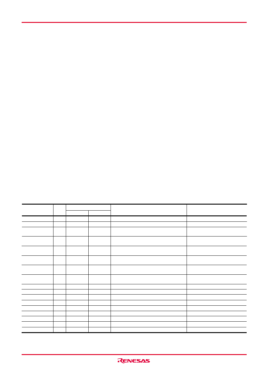
Table 6 Interrupt vector address and priority
Vector addresses (Note 1)
High-order
Priority
Low-order
Interrupt request generating conditions
Remarks
Interrupt source
FFFC16
FFFA16
FFF816
FFF616
FFF416
FFF216
FFF016
FFEE16
FFEC16
FFEA16
FFE816
FFE616
FFE416
FFE216
FFE016
FFDE16
FFDC16
FFFD16
FFFB16
FFF916
FFF716
FFF516
FFF316
FFF116
FFEF16
FFED16
FFEB16
FFE916
FFE716
FFE516
FFE316
FFE116
FFDF16
FFDD16
Note 1: Vector addressed contain internal jump destination addresses.
2: Reset function in the same way as an interrupt with the highest priority.
3: It is an interrupt which can use only for 36 pin version.
Non-maskable
Valid only when serial I/O1 is selected
Valid only when serial I/O1 is
selected
External interrupt
(active edge selectable)
External interrupt
(active edge selectable)
External interrupt (valid at falling)
External interrupt
(active edge selectable)
External interrupt
(active edge selectable)
STP release timer underflow
Non-maskable software interrupt
At reset input
At completion of serial I/O1 data receive
At completion of serial I/O1 transmit shift or
when transmit buffer is empty
At detection of either rising or falling edge of
INT0 input
At detection of either rising or falling edge of
INT1 input
At falling of conjunction of input logical level
for port P0 (at input)
At detection of either rising or falling edge of
CNTR0 input
At detection of either rising or falling edge of
CNTR1 input
At timer X underflow
At timer Y underflow
At timer Z underflow
At timer A underflow
At completion of transmit/receive shift
At completion of A/D conversion
At timer 1 underflow
Not available
At BRK instruction execution
1
2
3
4
5
6
7
8
9
10
11
12
13
14
15
16
17
Reset (Note 2)
Serial I/O1 receive
Serial I/O1 transmit
INT0
INT1 (Note 3)
Key-on wake-up
CNTR0
CNTR1
Timer X
Timer Y
Timer Z
Timer A
Serial I/O2
A/D conversion
Timer 1
Reserved area
BRK instruction
相关PDF资料 |
PDF描述 |
|---|---|
| M37540M2V-XXXFP | 8-BIT, MROM, 6 MHz, MICROCONTROLLER, PQFP32 |
| M37540M4V-XXXGP | 8-BIT, MROM, 6 MHz, MICROCONTROLLER, PDSO36 |
| M30624MGP-XXXGP | 16-BIT, MROM, 24 MHz, MICROCONTROLLER, PQFP100 |
| M37478E8SP | 8-BIT, OTPROM, 8 MHz, MICROCONTROLLER, PDIP42 |
| MC68HC908GR8AMDW | 8-BIT, FLASH, 8.2 MHz, MICROCONTROLLER, PDSO28 |
相关代理商/技术参数 |
参数描述 |
|---|---|
| M37540M2T-XXXGP | 制造商:RENESAS 制造商全称:Renesas Technology Corp 功能描述:8-BIT CISC SINGLE-CHIP MICROCOMPUTER 740 FAMILY / 740 SERIES |
| M37540M2V-XXXFP | 制造商:RENESAS 制造商全称:Renesas Technology Corp 功能描述:SINGLE-CHIP 8-BIT CMOS MICROCOMPUTER |
| M37540M2V-XXXGP | 制造商:RENESAS 制造商全称:Renesas Technology Corp 功能描述:8-BIT CISC SINGLE-CHIP MICROCOMPUTER 740 FAMILY / 740 SERIES |
| M37540M2-XXXFP | 制造商:RENESAS 制造商全称:Renesas Technology Corp 功能描述:8-BIT CISC SINGLE-CHIP MICROCOMPUTER 740 FAMILY / 740 SERIES |
| M37540M2-XXXGP | 制造商:RENESAS 制造商全称:Renesas Technology Corp 功能描述:SINGLE-CHIP 8-BIT CMOS MICROCOMPUTER |
发布紧急采购,3分钟左右您将得到回复。