- 您现在的位置:买卖IC网 > PDF目录98007 > M37906F8CSP 16-BIT, FLASH, 20 MHz, MICROCONTROLLER, PDIP42 PDF资料下载
参数资料
| 型号: | M37906F8CSP |
| 元件分类: | 微控制器/微处理器 |
| 英文描述: | 16-BIT, FLASH, 20 MHz, MICROCONTROLLER, PDIP42 |
| 封装: | 0.600 INCH, 1.78 MM PITCH, PLASTIC, SDIP-42 |
| 文件页数: | 15/37页 |
| 文件大小: | 352K |
| 代理商: | M37906F8CSP |
第1页第2页第3页第4页第5页第6页第7页第8页第9页第10页第11页第12页第13页第14页当前第15页第16页第17页第18页第19页第20页第21页第22页第23页第24页第25页第26页第27页第28页第29页第30页第31页第32页第33页第34页第35页第36页第37页
16-BIT CMOS MICROCOMPUTER
M37906F8CFP, M37906F8CSP
MITSUBISHI MICROCOMPUTERS
PRELIMINAR
Y
Notice:
This
is not
a final
specification.
Som
e param
etric
lim
its are
subject
to change.
19
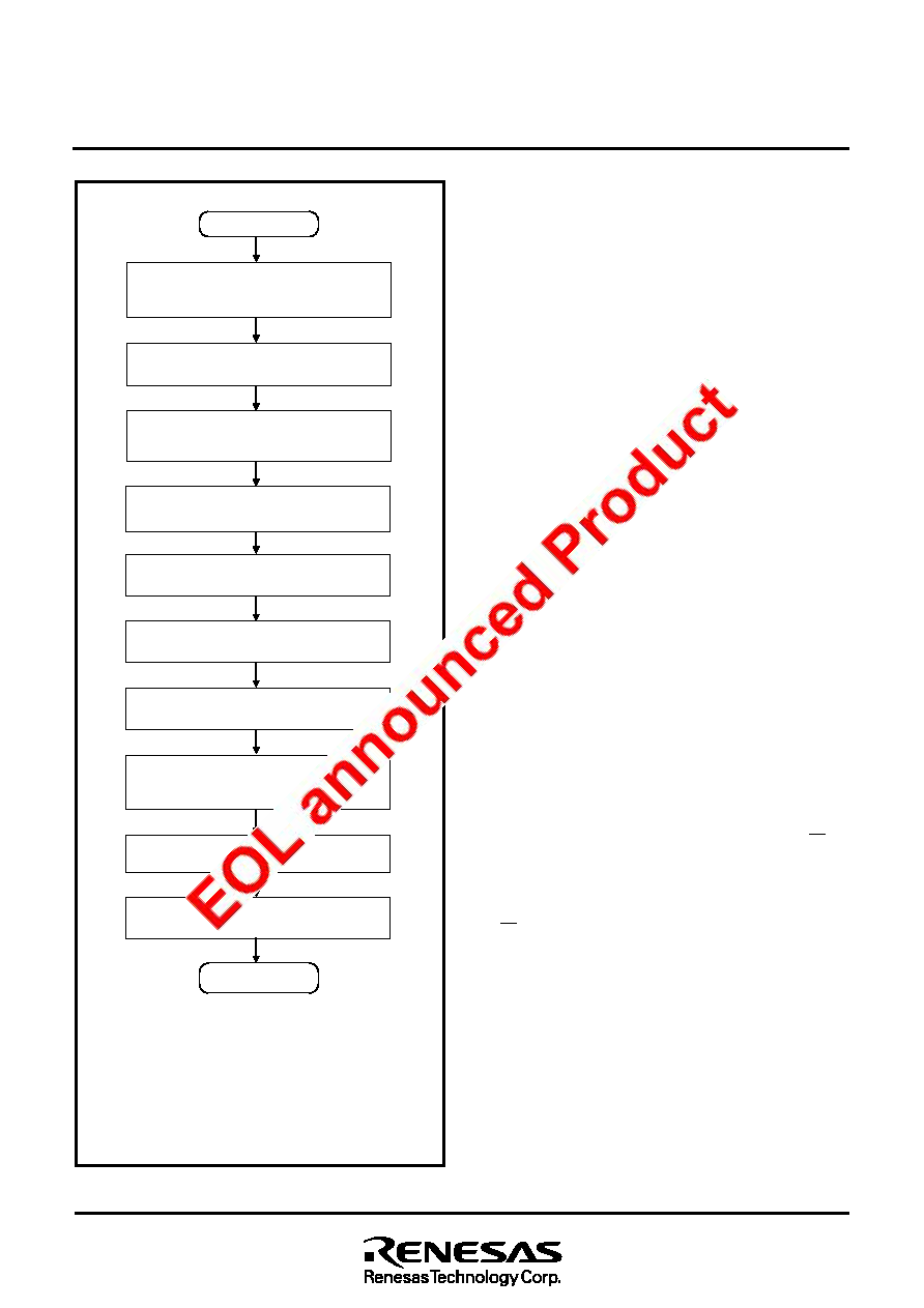
Fig. 8 CPU reprogramming mode set/termination flowchart
Software Commands
Table 2 lists the software commands.
By writing a software command after the CPU reprogramming mode
select bit has been set to “1”, erasing, programming, etc. can be
specified. Note that, at software commands’ input, the high-order
byte (D8–D15) is ignored. (Except for the write data at the 2nd cycle
of a programming command.)
Software commands are explained as below.
Read Array Command (FF16)
By writing command code “FF16” at the 1st bus cycle, the microcom-
puter enters the read array mode. If an address to be read is input in
the next or the following bus cycles, the contents at the specified ad-
dress are output to the data bus (D0 to D15) in a unit of 16 bits.
The read array mode is maintained until writing of another software
command.
Read Status Register Command (7016)
Writing command code “7016” at the 1st bus cycle outputs the con-
tents of the status register to the data bus (D0-D7) by a read at the
2nd bus cycle.
The status register is explained later.
Clear Status Register Command (5016)
This command clears two status bits (SR.4, 5) each of which is set
to “1” to indicate that the operation has been terminated by an error.
To clear these bits, write command code “5016” at the 1st bus cycle.
Programming Command (4016)
This command facilitates programming of 1 word (2 bytes) at a time.
To initiate programming, write command code “4016” at the 1st bus
cycle; when write data is written in a unit of 16 bits at the 2nd bus
cycle, the address is specified at the same time. Upon completion of
data writing, automatic programming (data programming and verifi-
cation) operation is started.
The completion of the automatic programming operation is con-
firmed by a read of the flash memory control register. The RY/BY sta-
tus bit of the flash memory control register goes “0” during the
automatic programming operation; and also, it goes “1” after the end
of it.
Before execution of the next command, be sure to confirm that the
RY/BY status bit is set to “1” (READY). During the automatic pro-
gramming operation, writing of commands and access to the flash
memory must not be performed.
When programming continuously, the programming command can
be executed with the read status register mode kept if there is no
programming error. Simultaneously with start of the automatic pro-
gramming, the read status register mode is automatically active. In
this case, the read status register mode is retained until the next read
array command (FF16) is written or until the reset is performed by
using the flash memory reset bit.
Reading out the status register after the automatic programming op-
eration is completed reports the result of it. For details, refer to the
section on the status register.
Figure 9 shows an example of the programming flowchart.
Additional programming to any word that has already been pro-
grammed is prohibited.
Completed
Start
Read array command is executed, or reset is
performed by setting the flash memory reset bit.
(Writing of “1”
→ Writing of “0”) (Note 2)
Single-chip mode,
Memory expansion mode,
or Boot mode
The processor mode register 1 is set (Note 1).
Flag I is set to “1”.
Operations such as erasing, programming are
executed by using software commands.
Jump to the above software in the internal RAM.
(The operations shown below will be executed by
the above software in this RAM.)
The user-original reprogramming control software
for the CPU reprogramming mode is transferred to
the internal RAM.
(Only in the boot mode.)
Writing of “0” to user ROM area select bit (Note 3).
Writing of “0” to the CPU reprogramming mode
select bit.
(Only in the boot mode.)
The user ROM area select bit is set to “1”.
Writing of “1” to the CPU reprogramming mode select bit.
(Writing of “0”
→ Writing of “1”)
Notes 1: The processor mode register 1’s bit 7 (address 5F16, the
internal ROM bus cycle select bit) must be “0” (bus cycle
= 3
φ).
2: To terminate the CPU reprogramming mode after the
erase and programming operations have been
completed, be sure to execute the read array command
or perform the flash memory reset operation.
3: This bit may remain “1”. However, if this bit is “1”, the
user ROM area access is specified.
相关PDF资料 |
PDF描述 |
|---|---|
| M37920S4CGP | 16-BIT, 20 MHz, MICROCONTROLLER, PQFP100 |
| M38184E8-XXXFP | 8-BIT, OTPROM, 6.3 MHz, MICROCONTROLLER, PQFP100 |
| M38184EA-XXXFP | 8-BIT, OTPROM, 6.3 MHz, MICROCONTROLLER, PQFP100 |
| M38184EAFP | 8-BIT, OTPROM, 8.4 MHz, MICROCONTROLLER, PQFP100 |
| M38222M2DXXXGP | 8-BIT, MROM, 8 MHz, MICROCONTROLLER, PQFP80 |
相关代理商/技术参数 |
参数描述 |
|---|---|
| M37906M4C-XXXFP | 制造商:RENESAS 制造商全称:Renesas Technology Corp 功能描述:16-BIT CMOS MICROCOMPUTER |
| M37906M4C-XXXSP | 制造商:RENESAS 制造商全称:Renesas Technology Corp 功能描述:16-BIT CMOS MICROCOMPUTER |
| M37906M4H-XXXFP | 制造商:RENESAS 制造商全称:Renesas Technology Corp 功能描述:16-BIT CMOS MICROCOMPUTER |
| M37906M6C-XXXFP | 制造商:RENESAS 制造商全称:Renesas Technology Corp 功能描述:16-BIT CMOS MICROCOMPUTER |
| M37906M6C-XXXSP | 制造商:RENESAS 制造商全称:Renesas Technology Corp 功能描述:16-BIT CMOS MICROCOMPUTER |
发布紧急采购,3分钟左右您将得到回复。