- 您现在的位置:买卖IC网 > PDF目录80355 > M38039G4H-XXXKP 8-BIT, MROM, 8.4 MHz, MICROCONTROLLER, PQFP64 PDF资料下载
参数资料
| 型号: | M38039G4H-XXXKP |
| 元件分类: | 微控制器/微处理器 |
| 英文描述: | 8-BIT, MROM, 8.4 MHz, MICROCONTROLLER, PQFP64 |
| 封装: | 14 X 14 MM, 0.80 MM PITCH, PLASTIC, LQFP-64 |
| 文件页数: | 86/105页 |
| 文件大小: | 1416K |
| 代理商: | M38039G4H-XXXKP |
第1页第2页第3页第4页第5页第6页第7页第8页第9页第10页第11页第12页第13页第14页第15页第16页第17页第18页第19页第20页第21页第22页第23页第24页第25页第26页第27页第28页第29页第30页第31页第32页第33页第34页第35页第36页第37页第38页第39页第40页第41页第42页第43页第44页第45页第46页第47页第48页第49页第50页第51页第52页第53页第54页第55页第56页第57页第58页第59页第60页第61页第62页第63页第64页第65页第66页第67页第68页第69页第70页第71页第72页第73页第74页第75页第76页第77页第78页第79页第80页第81页第82页第83页第84页第85页当前第86页第87页第88页第89页第90页第91页第92页第93页第94页第95页第96页第97页第98页第99页第100页第101页第102页第103页第104页第105页
REJ03B0166-0113 Rev.1.13
Aug 21, 2009
Page 79 of 100
3803 Group (Spec.H QzROM version)
6. Serial Interface
In clock synchronous serial I/O, if the receive side is using an
external clock and it is to output the SRDY signal, set the transmit
enable bit, the receive enable bit, and the SRDY output enable bit
to “1”.
Serial I/O1 continues to output the final bit from the TXD1 pin
after transmission is completed. SOUT2 pin for serial I/O2 goes to
high impedance after transfer is completed.
When in serial I/Os 1 and 3 (clock-synchronous mode) or in
serial I/O2, an external clock is used as synchronous clock, write
transmission data to the transmit buffer register or serial I/O2
register, during transfer clock is “H”.
7. A/D Converter
The comparator uses capacitive coupling amplifier whose charge
will be lost if the clock frequency is too low.
Therefore, make sure that f(XIN) in the middle/high-speed mode
is at least on 500 kHz during an A/D conversion.
Do not execute the STP instruction during an A/D conversion.
8. D/A Converter
The accuracy of the D/A converter becomes rapidly poor under
the VCC = 4.0 V or less condition; a supply voltage of VCC
≥ 4.0
V is recommended. When a D/A converter is not used, set all
values of DAi conversion registers (i=1, 2) to “0016”.
9. Instruction Execution Time
The instruction execution time is obtained by multiplying the
period of the internal clock
φ by the number of cycles needed to
execute an instruction.
The number of cycles required to execute an instruction is shown
in the list of machine instructions.
The period of the internal clock
φ is double of the XIN period in
high-speed mode.
10.Reserved Area, Reserved Bit
Do not write any data to the reserved area in the SFR area and the
special page. (Do not change the contents after reset.)
11.CPU Mode Register
Be sure to fix bit 3 of the CPU mode register (address 003B16) to
“1”.
COUNTERMEASURES AGAINST NOISE
(1) Shortest wiring length
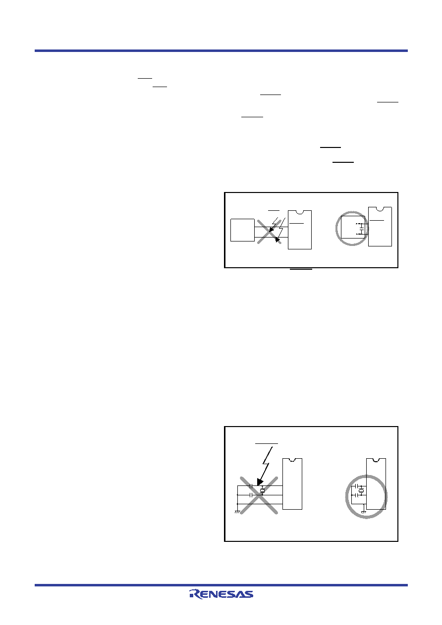
1. Wiring for RESET pin
Make the length of wiring which is connected to the RESET
pin as short as possible. Especially, connect a capacitor across
the RESET pin and the VSS pin with the shortest possible
wiring (within 20 mm).
Reason
The width of a pulse input into the RESET pin is determined by
the timing necessary conditions. If noise having a shorter pulse
width than the standard is input to the RESET pin, the reset is
released before the internal state of the microcomputer is
completely initialized. This may cause a program runaway.
Fig. 76 Wiring for the RESET pin
2. Wiring for clock input/output pins
Make the length of wiring which is connected to clock I/O
pins as short as possible.
Make the length of wiring (within 20 mm) across the
grounding lead of a capacitor which is connected to an
oscillator and the VSS pin of a microcomputer as short as
possible.
Separate the VSS pattern only for oscillation from other VSS
patterns.
Reason
If noise enters clock I/O pins, clock waveforms may be
deformed.
This may cause a program failure or program runaway. Also, if a
potential difference is caused by the noise between the VSS level
of a microcomputer and the VSS level of an oscillator, the correct
clock will not be input in the microcomputer.
Fig. 77 Wiring for clock I/O pins
RESET
Reset
circuit
Noise
VSS
N.G.
Reset
circuit
VSS
RESET
VSS
O.K.
Noise
XIN
XOUT
VSS
N.G.
XIN
XOUT
VSS
O.K.
相关PDF资料 |
PDF描述 |
|---|---|
| M38044M4-XXXFP | 8-BIT, MROM, 8.4 MHz, MICROCONTROLLER, PQFP64 |
| M38517F8SP | 8-BIT, FLASH, 4 MHz, MICROCONTROLLER, PDIP42 |
| M38D24G6-XXXFP | 8-BIT, FLASH, 6.25 MHz, MICROCONTROLLER, PQFP64 |
| M102E1000.0000DK | 1000 MHz, OTHER CLOCK GENERATOR, MDIP24 |
| M38022M4-XXXSP | 8-BIT, MROM, 8 MHz, MICROCONTROLLER, PDIP64 |
相关代理商/技术参数 |
参数描述 |
|---|---|
| M38039G6HHP#U0 | 功能描述:IC 740/3803 MCU QZROM 64LQFP RoHS:是 类别:集成电路 (IC) >> 嵌入式 - 微控制器, 系列:740/38000 标准包装:250 系列:80C 核心处理器:8051 芯体尺寸:8-位 速度:16MHz 连通性:EBI/EMI,I²C,UART/USART 外围设备:POR,PWM,WDT 输入/输出数:40 程序存储器容量:- 程序存储器类型:ROMless EEPROM 大小:- RAM 容量:256 x 8 电压 - 电源 (Vcc/Vdd):4.5 V ~ 5.5 V 数据转换器:A/D 8x10b 振荡器型:内部 工作温度:-40°C ~ 85°C 封装/外壳:68-LCC(J 形引线) 包装:带卷 (TR) |
| M38039G6HKP#U0 | 功能描述:IC 740/3803 MCU QZROM 64LQFP RoHS:是 类别:集成电路 (IC) >> 嵌入式 - 微控制器, 系列:740/38000 标准包装:250 系列:80C 核心处理器:8051 芯体尺寸:8-位 速度:16MHz 连通性:EBI/EMI,I²C,UART/USART 外围设备:POR,PWM,WDT 输入/输出数:40 程序存储器容量:- 程序存储器类型:ROMless EEPROM 大小:- RAM 容量:256 x 8 电压 - 电源 (Vcc/Vdd):4.5 V ~ 5.5 V 数据转换器:A/D 8x10b 振荡器型:内部 工作温度:-40°C ~ 85°C 封装/外壳:68-LCC(J 形引线) 包装:带卷 (TR) |
| M38039G6HSP#U0 | 功能描述:IC 740/3803 MCU QZROM 64DIP RoHS:是 类别:集成电路 (IC) >> 嵌入式 - 微控制器, 系列:740/38000 标准包装:250 系列:80C 核心处理器:8051 芯体尺寸:8-位 速度:16MHz 连通性:EBI/EMI,I²C,UART/USART 外围设备:POR,PWM,WDT 输入/输出数:40 程序存储器容量:- 程序存储器类型:ROMless EEPROM 大小:- RAM 容量:256 x 8 电压 - 电源 (Vcc/Vdd):4.5 V ~ 5.5 V 数据转换器:A/D 8x10b 振荡器型:内部 工作温度:-40°C ~ 85°C 封装/外壳:68-LCC(J 形引线) 包装:带卷 (TR) |
| M38039G8HHP#U0 | 功能描述:IC 740/3803 MCU QZROM 64LQFP RoHS:是 类别:集成电路 (IC) >> 嵌入式 - 微控制器, 系列:740/38000 标准包装:250 系列:80C 核心处理器:8051 芯体尺寸:8-位 速度:16MHz 连通性:EBI/EMI,I²C,UART/USART 外围设备:POR,PWM,WDT 输入/输出数:40 程序存储器容量:- 程序存储器类型:ROMless EEPROM 大小:- RAM 容量:256 x 8 电压 - 电源 (Vcc/Vdd):4.5 V ~ 5.5 V 数据转换器:A/D 8x10b 振荡器型:内部 工作温度:-40°C ~ 85°C 封装/外壳:68-LCC(J 形引线) 包装:带卷 (TR) |
| M38039G8HKP#U0 | 功能描述:IC 740/3803 MCU QZROM 64LQFP RoHS:是 类别:集成电路 (IC) >> 嵌入式 - 微控制器, 系列:740/38000 标准包装:250 系列:80C 核心处理器:8051 芯体尺寸:8-位 速度:16MHz 连通性:EBI/EMI,I²C,UART/USART 外围设备:POR,PWM,WDT 输入/输出数:40 程序存储器容量:- 程序存储器类型:ROMless EEPROM 大小:- RAM 容量:256 x 8 电压 - 电源 (Vcc/Vdd):4.5 V ~ 5.5 V 数据转换器:A/D 8x10b 振荡器型:内部 工作温度:-40°C ~ 85°C 封装/外壳:68-LCC(J 形引线) 包装:带卷 (TR) |
发布紧急采购,3分钟左右您将得到回复。