- 您现在的位置:买卖IC网 > PDF目录80355 > M38039G4H-XXXKP 8-BIT, MROM, 8.4 MHz, MICROCONTROLLER, PQFP64 PDF资料下载
参数资料
| 型号: | M38039G4H-XXXKP |
| 元件分类: | 微控制器/微处理器 |
| 英文描述: | 8-BIT, MROM, 8.4 MHz, MICROCONTROLLER, PQFP64 |
| 封装: | 14 X 14 MM, 0.80 MM PITCH, PLASTIC, LQFP-64 |
| 文件页数: | 91/105页 |
| 文件大小: | 1416K |
| 代理商: | M38039G4H-XXXKP |
第1页第2页第3页第4页第5页第6页第7页第8页第9页第10页第11页第12页第13页第14页第15页第16页第17页第18页第19页第20页第21页第22页第23页第24页第25页第26页第27页第28页第29页第30页第31页第32页第33页第34页第35页第36页第37页第38页第39页第40页第41页第42页第43页第44页第45页第46页第47页第48页第49页第50页第51页第52页第53页第54页第55页第56页第57页第58页第59页第60页第61页第62页第63页第64页第65页第66页第67页第68页第69页第70页第71页第72页第73页第74页第75页第76页第77页第78页第79页第80页第81页第82页第83页第84页第85页第86页第87页第88页第89页第90页当前第91页第92页第93页第94页第95页第96页第97页第98页第99页第100页第101页第102页第103页第104页第105页
REJ03B0166-0113 Rev.1.13
Aug 21, 2009
Page 84 of 100
3803 Group (Spec.H QzROM version)
2. Notes when selecting clock asynchronous serial I/O
(1) Stop of transmission operation
Clear the transmit enable bit to “0” (transmit disabled). The
transmission operation does not stop by clearing the serial I/Oi
enable bit (i = 1, 3) to “0”.
<Reason>
This is the same as (1) in 1.
(2) Stop of receive operation
Clear the receive enable bit to “0” (receive disabled).
(3) Stop of transmit/receive operation
Only transmission operation is stopped.
Clear the transmit enable bit to “0” (transmit disabled). The
transmission operation does not stop by clearing the serial I/Oi
enable bit (i = 1, 3) to “0”.
<Reason>
This is the same as (1) in 1.
Only receive operation is stopped.
Clear the receive enable bit to “0” (receive disabled).
3. SRDYi (i = 1, 3) output of reception side
When signals are output from the SRDYi pin on the reception side
by using an external clock in the clock synchronous serial I/O
mode, set all of the receive enable bit, the SRDYi output enable
bit, and the transmit enable bit to “1” (transmit enabled).
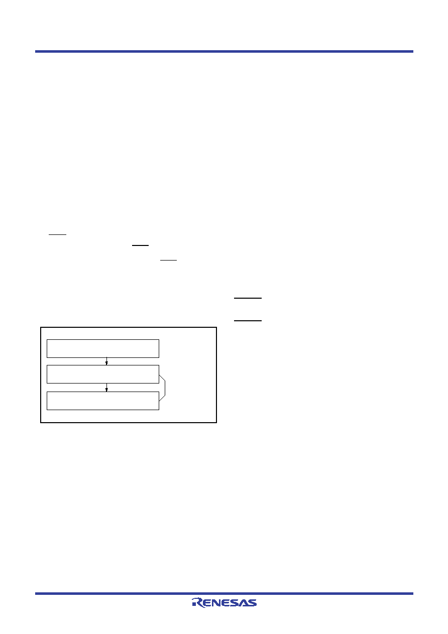
4. Setting serial I/Oi (i = 1, 3) control register again
Set the serial I/Oi control register again after the transmission
and the reception circuits are reset by clearing both the transmit
enable bit and the receive enable bit to “0.”
Fig 82. Sequence of setting serial I/Oi (i = 1, 3) control
register again
5. Data transmission control with referring to transmit
shift register completion flag
After the transmit data is written to the transmit buffer register,
the transmit shift register completion flag changes from “1” to
“0” with a delay of 0.5 to 1.5 shift clocks. When data
transmission is controlled with referring to the flag after writing
the data to the transmit buffer register, note the delay.
6. Transmission control when external clock is selected
When an external clock is used as the synchronous clock for data
transmission, set the transmit enable bit to “1” at “H” of the
SCLKi (i = 1, 3) input level. Also, write the transmit data to the
transmit buffer register at “H” of the SCLKi input level.
7. Transmit interrupt request when transmit enable bit
is set
When using the transmit interrupt, take the following sequence.
(1) Set the serial I/Oi transmit interrupt enable bit (i = 1, 3) to
“0” (disabled).
(2) Set the transmit enable bit to “1”.
(3) Set the serial I/Oi transmit interrupt request bit (i = 1, 3) to
“0” after 1 or more instruction has executed.
(4) Set the serial I/Oi transmit interrupt enable bit (i = 1, 3) to
“1” (enabled).
<Reason>
When the transmission enable bit is set to “1”, the transmit buffer
empty flag and transmit shift register shift completion flag are
also set to “1”.
Therefore, regardless of selecting which timing for the
generating of transmit interrupts, the interrupt request is
generated and the transmit interrupt request bit is set at this point.
8. Writing to baud rate generator i (BRGi) (i = 1, 3)
Write data to the baud rate generator i (BRGi) (i = 1, 3) while the
transmission/reception operation is stopped.
Notes on PWM
The PWM starts from “H” level after the PWM enable bit is set
to enable and “L” level is temporarily output from the PWM pin.
The length of this “L” level output is as follows:
n + 1
2
× f(XIN)
(s)
(Count source selection bit = “0”,
where n is the value set in the prescaler)
n + 1
f(XIN)
(s)
(Count source selection bit = “1”,
where n is the value set in the prescaler)
Notes on A/D Converter
1. Analog input pin
Make the signal source impedance for analog input low, or equip
an analog input pin with an external capacitor of 0.01
F to 1 F.
Further, be sure to verify the operation of application products on
the user side.
<Reason>
An analog input pin includes the capacitor for analog voltage
comparison. Accordingly, when signals from signal source with
high impedance are input to an analog input pin, charge and
discharge noise generates. This may cause the A/D conversion
precision to be worse.
2. A/D converter power source pin
The AVSS pin is A/D converter power source pins. Regardless of
using the A/D conversion function or not, connect it as following:
AVSS: Connect to the VSS line
<Reason>
If the AVSS pin is opened, the microcomputer may have a failure
because of noise or others.
Can be set with the
LDM instruction at
the same time
Set the bits 0 to 3 and bit 6 of the serial I/Oi
control register
Clear both the transmit enable bit (TE) and
the receive enable bit (RE) to “0”
Set both the transmit enable bit (TE) and the
receive enable bit (RE), or one of them to “1”
相关PDF资料 |
PDF描述 |
|---|---|
| M38044M4-XXXFP | 8-BIT, MROM, 8.4 MHz, MICROCONTROLLER, PQFP64 |
| M38517F8SP | 8-BIT, FLASH, 4 MHz, MICROCONTROLLER, PDIP42 |
| M38D24G6-XXXFP | 8-BIT, FLASH, 6.25 MHz, MICROCONTROLLER, PQFP64 |
| M102E1000.0000DK | 1000 MHz, OTHER CLOCK GENERATOR, MDIP24 |
| M38022M4-XXXSP | 8-BIT, MROM, 8 MHz, MICROCONTROLLER, PDIP64 |
相关代理商/技术参数 |
参数描述 |
|---|---|
| M38039G6HHP#U0 | 功能描述:IC 740/3803 MCU QZROM 64LQFP RoHS:是 类别:集成电路 (IC) >> 嵌入式 - 微控制器, 系列:740/38000 标准包装:250 系列:80C 核心处理器:8051 芯体尺寸:8-位 速度:16MHz 连通性:EBI/EMI,I²C,UART/USART 外围设备:POR,PWM,WDT 输入/输出数:40 程序存储器容量:- 程序存储器类型:ROMless EEPROM 大小:- RAM 容量:256 x 8 电压 - 电源 (Vcc/Vdd):4.5 V ~ 5.5 V 数据转换器:A/D 8x10b 振荡器型:内部 工作温度:-40°C ~ 85°C 封装/外壳:68-LCC(J 形引线) 包装:带卷 (TR) |
| M38039G6HKP#U0 | 功能描述:IC 740/3803 MCU QZROM 64LQFP RoHS:是 类别:集成电路 (IC) >> 嵌入式 - 微控制器, 系列:740/38000 标准包装:250 系列:80C 核心处理器:8051 芯体尺寸:8-位 速度:16MHz 连通性:EBI/EMI,I²C,UART/USART 外围设备:POR,PWM,WDT 输入/输出数:40 程序存储器容量:- 程序存储器类型:ROMless EEPROM 大小:- RAM 容量:256 x 8 电压 - 电源 (Vcc/Vdd):4.5 V ~ 5.5 V 数据转换器:A/D 8x10b 振荡器型:内部 工作温度:-40°C ~ 85°C 封装/外壳:68-LCC(J 形引线) 包装:带卷 (TR) |
| M38039G6HSP#U0 | 功能描述:IC 740/3803 MCU QZROM 64DIP RoHS:是 类别:集成电路 (IC) >> 嵌入式 - 微控制器, 系列:740/38000 标准包装:250 系列:80C 核心处理器:8051 芯体尺寸:8-位 速度:16MHz 连通性:EBI/EMI,I²C,UART/USART 外围设备:POR,PWM,WDT 输入/输出数:40 程序存储器容量:- 程序存储器类型:ROMless EEPROM 大小:- RAM 容量:256 x 8 电压 - 电源 (Vcc/Vdd):4.5 V ~ 5.5 V 数据转换器:A/D 8x10b 振荡器型:内部 工作温度:-40°C ~ 85°C 封装/外壳:68-LCC(J 形引线) 包装:带卷 (TR) |
| M38039G8HHP#U0 | 功能描述:IC 740/3803 MCU QZROM 64LQFP RoHS:是 类别:集成电路 (IC) >> 嵌入式 - 微控制器, 系列:740/38000 标准包装:250 系列:80C 核心处理器:8051 芯体尺寸:8-位 速度:16MHz 连通性:EBI/EMI,I²C,UART/USART 外围设备:POR,PWM,WDT 输入/输出数:40 程序存储器容量:- 程序存储器类型:ROMless EEPROM 大小:- RAM 容量:256 x 8 电压 - 电源 (Vcc/Vdd):4.5 V ~ 5.5 V 数据转换器:A/D 8x10b 振荡器型:内部 工作温度:-40°C ~ 85°C 封装/外壳:68-LCC(J 形引线) 包装:带卷 (TR) |
| M38039G8HKP#U0 | 功能描述:IC 740/3803 MCU QZROM 64LQFP RoHS:是 类别:集成电路 (IC) >> 嵌入式 - 微控制器, 系列:740/38000 标准包装:250 系列:80C 核心处理器:8051 芯体尺寸:8-位 速度:16MHz 连通性:EBI/EMI,I²C,UART/USART 外围设备:POR,PWM,WDT 输入/输出数:40 程序存储器容量:- 程序存储器类型:ROMless EEPROM 大小:- RAM 容量:256 x 8 电压 - 电源 (Vcc/Vdd):4.5 V ~ 5.5 V 数据转换器:A/D 8x10b 振荡器型:内部 工作温度:-40°C ~ 85°C 封装/外壳:68-LCC(J 形引线) 包装:带卷 (TR) |
发布紧急采购,3分钟左右您将得到回复。