- 您现在的位置:买卖IC网 > PDF目录80462 > M38507F8AFP 8-BIT, FLASH, 6.25 MHz, MICROCONTROLLER, PDSO42 PDF资料下载
参数资料
| 型号: | M38507F8AFP |
| 元件分类: | 微控制器/微处理器 |
| 英文描述: | 8-BIT, FLASH, 6.25 MHz, MICROCONTROLLER, PDSO42 |
| 封装: | 8.40 X 17.50 MM, 0.80 MM PITCH, PLASTIC, SSOP-42 |
| 文件页数: | 23/59页 |
| 文件大小: | 885K |
| 代理商: | M38507F8AFP |
第1页第2页第3页第4页第5页第6页第7页第8页第9页第10页第11页第12页第13页第14页第15页第16页第17页第18页第19页第20页第21页第22页当前第23页第24页第25页第26页第27页第28页第29页第30页第31页第32页第33页第34页第35页第36页第37页第38页第39页第40页第41页第42页第43页第44页第45页第46页第47页第48页第49页第50页第51页第52页第53页第54页第55页第56页第57页第58页第59页
Rev.2.13
Apr 17, 2009
Page 3 of 56
REJ03B0125-0213
3850 Group (Spec.A QzROM version)
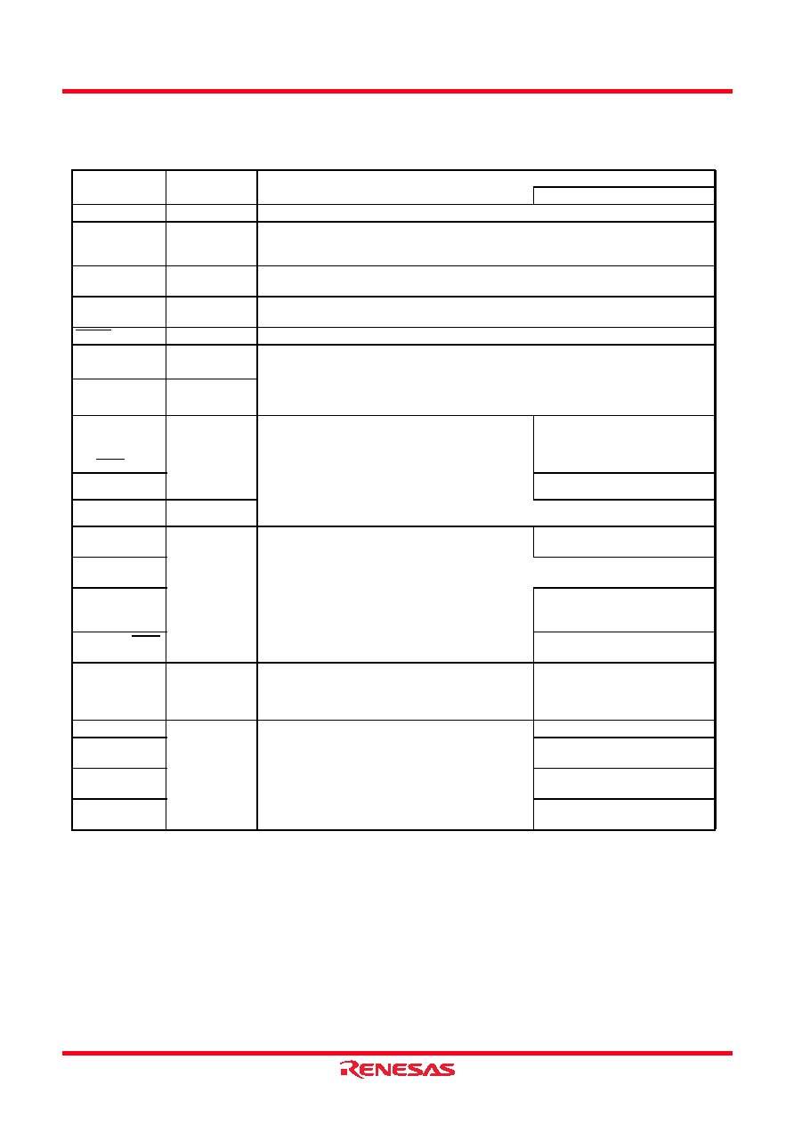
PIN DESCRIPTION
Table 1
Pin description
Pin
Name
Function
Function except a port function
VCC, VSS
Power source
Apply voltage of 1.8 V
5.5 V to VCC, and 0 V to VSS.
CNVSS
CNVSS input
This pin controls the operation mode of the chip and is shared with the VPP pin which is the
power source input pin for programming the built-in QzROM.
Normally connected to VSS.
VREF
Reference
voltage
Reference voltage input pin for A/D converter.
AVSS
Analog power
source
Analog power source input pin for A/D converter.
Connect to VSS.
RESET
Reset input
Reset input pin for active “L”.
XIN
Clock input
Input and output pins for the clock generating circuit.
Connect a ceramic resonator or quartz-crystal oscillator between the XIN and XOUT pins to set
the oscillation frequency.
When an external clock is used, connect the clock source to the XIN pin and leave the XOUT pin
open.
XOUT
Clock output
P00/SIN2
P01/SOUT2
P02/SCLK2
P03/SRDY2
I/O port P0
8-bit CMOS I/O port.
I/O direction register allows each pin to be individually
programmed as either input or output.
CMOS compatible input level.
CMOS 3-state output structure.
Pull-up control is enabled in a byte unit.
P10 to P17 (8 bits) are enabled to output large current
for LED drive.
Serial I/O2 function pin
P04/AN5
P07/AN8
A/D converter input pin
P10-P17
I/O port P1
P20/XCOUT
P21/XCIN
I/O port P2
8-bit CMOS I/O port.
I/O direction register allows each pin to be individually
programmed as either input or output.
CMOS compatible input level.
P20, P21, P24, to P27: CMOS3-state output structure.
P22, P23: N-channel open-drain structure.
Pull-up control of P20, P21, P24
P27 is enabled in a
byte unit.
Sub-clock generating circuit I/O
pins (connect a resonator)
P22
P23
P24/RXD
P25/TXD
P26/SCLK1
Serial I/O1 function pin
P27/CNTR0/SRDY1
Serial I/O1 function pin
Timer X function pin
P30/AN0
P34/AN4 I/O port P3
5-bit CMOS I/O port with the same function as port P0.
CMOS compatible input level.
CMOS 3-state output structure.
Pull-up control is enabled in a bit unit.
A/D converter input pin
P40/CNTR1
I/O port P4
5-bit CMOS I/O port with the same function as port P0.
CMOS compatible input level.
CMOS 3-state output structure.
Pull-up control is enabled in a bit unit.
Timer Y function pin
P41/INT0
P42/INT1
Interrupt input pins
P43/INT2/SCMP2
Interrupt input pin
SCMP2 output pin
P44/INT3/PWM
Interrupt input pin
PWM output pin
相关PDF资料 |
PDF描述 |
|---|---|
| MC68EN360RC33 | RISC MICROCONTROLLER, CPGA241 |
| MC56F8365MFG60 | 4-BIT, 120 MHz, OTHER DSP, PQFP128 |
| MPC8378ECVRANDA | 32-BIT, 266 MHz, MICROPROCESSOR, PBGA689 |
| MB95F214KPH-G-SNE2 | 8-BIT, FLASH, MICROCONTROLLER, PDIP8 |
| MC9S12XS128J1VALR | 16-BIT, FLASH, 40 MHz, MICROCONTROLLER, PQFP112 |
相关代理商/技术参数 |
参数描述 |
|---|---|
| M38507F8AFP#U1 | 功能描述:IC 740/3850 MCU FLASH 42SSOP RoHS:是 类别:集成电路 (IC) >> 嵌入式 - 微控制器, 系列:740/38000 产品培训模块:CAN Basics Part-1 CAN Basics Part-2 Electromagnetic Noise Reduction Techniques Part 1 M16C Product Overview Part 1 M16C Product Overview Part 2 标准包装:1 系列:M16C™ M32C/80/87 核心处理器:M32C/80 芯体尺寸:16/32-位 速度:32MHz 连通性:EBI/EMI,I²C,IEBus,IrDA,SIO,UART/USART 外围设备:DMA,POR,PWM,WDT 输入/输出数:121 程序存储器容量:384KB(384K x 8) 程序存储器类型:闪存 EEPROM 大小:- RAM 容量:24K x 8 电压 - 电源 (Vcc/Vdd):3 V ~ 5.5 V 数据转换器:A/D 34x10b,D/A 2x8b 振荡器型:内部 工作温度:-20°C ~ 85°C 封装/外壳:144-LQFP 包装:托盘 产品目录页面:749 (CN2011-ZH PDF) 配用:R0K330879S001BE-ND - KIT DEV RSK M32C/87 |
| M38507F8AFP#W1 | 制造商:Renesas Electronics Corporation 功能描述:MCU 3/5V 32K PB-FREE 42-SSOP T&R - Tape and Reel |
| M38507F8FP | 制造商:Renesas Electronics Corporation 功能描述:MCU 8-Bit 740 CISC 32KB Flash 5V 42-Pin SSOP 制造商:Renesas Electronics Corporation 功能描述:MCU 8BIT 740 CISC 32KB FLASH 5V 42SSOP - Trays |
| M38507F8FP#U1 | 制造商:Renesas Electronics Corporation 功能描述:MCU 8BIT 740 CISC 32KB FLASH 5V 42SSOP - Trays |
| M38507F8FP#W1 | 制造商:Renesas Electronics Corporation 功能描述:FLASH 8-BIT 2.7 TO 5.5V PBFREE |
发布紧急采购,3分钟左右您将得到回复。