- 您现在的位置:买卖IC网 > PDF目录299434 > M39208-15WNB1 (STMICROELECTRONICS) 256K X 8 FLASH 2.7V PROM, 150 ns, PDSO32 PDF资料下载
参数资料
| 型号: | M39208-15WNB1 |
| 厂商: | STMICROELECTRONICS |
| 元件分类: | PROM |
| 英文描述: | 256K X 8 FLASH 2.7V PROM, 150 ns, PDSO32 |
| 封装: | 8 X 14 MM, PLASTIC, TSOP-32 |
| 文件页数: | 25/30页 |
| 文件大小: | 218K |
| 代理商: | M39208-15WNB1 |
第1页第2页第3页第4页第5页第6页第7页第8页第9页第10页第11页第12页第13页第14页第15页第16页第17页第18页第19页第20页第21页第22页第23页第24页当前第25页第26页第27页第28页第29页第30页
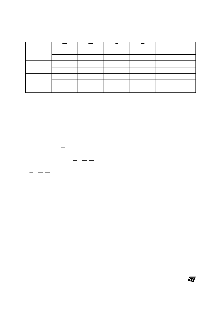
Operation
EF
EE
G
W
DQ0 - DQ7
Read
VIL
VIH
VIL
VIH
Read in Flash Block
VIH
VIL
VIH
Read in EEPROM Block
Write
VIL
VIH
VIL
Write in Flash Block
VIH
VIL
VIH
VIL
Write in EEPROM Block
Output Disable
VIL
VIH
XHi-Z
VIH
VIL
VIH
XHi-Z
Standby
VIH
XX
Hi-Z
Note: X = VIL or VIH.
Table 3. Basic Operations
Write. A Write operation can be used for two goals:
– either write data in the EEPROM memory block
– or enter a sequence of bytes composing an
instruction.
The reader should note that Programming a Flash
byte is an instruction (see Instructions paragraph).
Writing data requires:
– the Chip Enable (either EE or EF) to be Low
– the Write Enable (W) to be Low with Output
Enable (G) High.
Addresses in Flash block (or EEPROM block) are
latched on the falling edge of W or EF (EE) which-
ever occurs last; the data to be written in Flash
block (EEPROM block) is latched on the rising edge
of W or EF (EE) whichever occurs first.
Specific Read and Write Operations. Device
specific data is accessed through operations de-
coding the VID level applied on A9 (VID = 12V +
0.5V) and the logic levels applied on address inputs
(A0, A1, A6). These specific operations are:
– Read the Manufacturer identifier
– Read the Device identifier
– Define the Flash Sector protection
– Read the EEPROM identifier
– Write the EEPROM identifier
Note: The OTP row (64 bytes) is accessed with a
specific software sequence detailed in the para-
graph "Write in OTP row".
Instructions
An instruction is defined as a sequence of specific
Write operations. Each received byte is sequen-
tially decoded (and not executed as standard Write
operations) and the instruction is executed when
the correct number of bytes are properly received
and the time between two consecutive bytes is
shorter than the time-out value.
The sequencing of any instruction must be followed
exactly, any invalid combination of instruction bytes
or time-out between two consecutive bytes will
reset the device logic into a Read memory state
(when addressing the Flash block) or directly de-
coded as a single operation when addressing the
EEPROM block.
The M39208 set of instructions includes:
– Program a byte in the Flash block
– Read a Flash sector protection status
– Erase instructions: Flash Sector Erase, Flash
Block Erase, Flash Sector Erase Suspend, Flash
Sector Erase Resume
– EEPROM power down
– Deep power down
– Set/Reset the EEPROM software write protec-
tion (SDP)
– OTP row access
– Reset and Return
– Read identifiers: read the manufacturer identi-
fier, Read the Flash block identifier
These instructions are detailed in Table 4.
For efficient decoding of the instruction, the two first
bytes of an instruction are the coded cycles and are
followed by a command byte or a confirmation byte.
The coded cycles consist of writing the data AAh at
address 5555h during the first cycle and data 55h
at address 2AAAh during the second cycle.
In the specific case of the Erase instruction, the
instruction expects confirmation by two additional
coded cycles.
4/30
M39208
相关PDF资料 |
PDF描述 |
|---|---|
| M3933/10-17N | 0 MHz - 18000 MHz RF/MICROWAVE FIXED ATTENUATOR |
| M3933/25-65N | 0 MHz - 18000 MHz RF/MICROWAVE FIXED ATTENUATOR |
| M3933/10-16S | 0 MHz - 18000 MHz RF/MICROWAVE FIXED ATTENUATOR |
| M3933/14-23S | 0 MHz - 12400 MHz RF/MICROWAVE FIXED ATTENUATOR |
| M3933/25-31S | 0 MHz - 18000 MHz RF/MICROWAVE FIXED ATTENUATOR |
相关代理商/技术参数 |
参数描述 |
|---|---|
| M39208-15WNB1T | 制造商:STMICROELECTRONICS 制造商全称:STMicroelectronics 功能描述:Single Chip 2 Mbit Flash and 64 Kbit Parallel EEPROM Memory |
| M39208-15WNB5T | 制造商:STMICROELECTRONICS 制造商全称:STMicroelectronics 功能描述:Single Chip 2 Mbit Flash and 64 Kbit Parallel EEPROM Memory |
| M39208-15WNB6T | 制造商:STMICROELECTRONICS 制造商全称:STMicroelectronics 功能描述:Single Chip 2 Mbit Flash and 64 Kbit Parallel EEPROM Memory |
| M39208NA | 制造商:STMICROELECTRONICS 制造商全称:STMicroelectronics 功能描述:Single Chip 2 Mbit Flash and 64 Kbit Parallel EEPROM Memory |
| M39208NB | 制造商:STMICROELECTRONICS 制造商全称:STMicroelectronics 功能描述:Single Chip 2 Mbit Flash and 64 Kbit Parallel EEPROM Memory |
发布紧急采购,3分钟左右您将得到回复。