- 您现在的位置:买卖IC网 > PDF目录299434 > M39208-15WNB1 (STMICROELECTRONICS) 256K X 8 FLASH 2.7V PROM, 150 ns, PDSO32 PDF资料下载
参数资料
| 型号: | M39208-15WNB1 |
| 厂商: | STMICROELECTRONICS |
| 元件分类: | PROM |
| 英文描述: | 256K X 8 FLASH 2.7V PROM, 150 ns, PDSO32 |
| 封装: | 8 X 14 MM, PLASTIC, TSOP-32 |
| 文件页数: | 29/30页 |
| 文件大小: | 218K |
| 代理商: | M39208-15WNB1 |
第1页第2页第3页第4页第5页第6页第7页第8页第9页第10页第11页第12页第13页第14页第15页第16页第17页第18页第19页第20页第21页第22页第23页第24页第25页第26页第27页第28页当前第29页第30页
– if all the Flash sectors selected for erasure
are protected, DQ6 will toggle to ’0’ for about
100
s, and then return to the previous ad-
dressed byte.
– if all sectors are protected, the Bulk Erase in-
struction is ignored.
Error flag, DQ5 (Flash block only). This bit is set
to ’1’ when there is a failure during either a Flash
byte programming or a Sector erase or the Bulk
Erase.
In case of error in Flash sector erase or byte
program, the Flash sector in which the error oc-
curred or to which the programmed byte belongs,
must not be used any longer (other Flash sectors
may still be used). The Error bit resets after Reset
instruction.
During a correct Program or Erase, the Error bit will
set to ’0’.
Erase Time-out flag, DQ3 (Flash block only).
The Erase Timer bit reflects the time-out period
allowed between two consecutive Sector Erase
instructions. The Erase timer bit is set to ’0’ after a
Sector Erase instruction for a time period of 100
s
± 20% unless an additional Sector Erase instruction
is decoded. After this time period or when the
additional Sector Erase instruction is decoded,
DQ3 is set to ’1’.
WRITE a BYTE (or a PAGE) in EEPROM
It should be noticed that writing in the EEPROM
block is an operation, it is not an instruction (as for
Programming a byte in the Flash block).
Write a Byte in EEPROM Block
A write operation is initiated when Chip Enable EE
is Low and Write Enable W is Low with Output
Enable G High. Addresses are latched on the falling
edge of W, EE whichever occurs last.
Once initiated, the write operation is internally
timed until completion, that is during a time tW.
The status of the write operation can be found by
reading the Data Polling and Toggle bits (as de-
tailed in the READ chapter) or the Ready/Busy
output. This Ready/Busy output is driven low from
the write of the byte being written until the comple-
tion of the internal Write sequence.
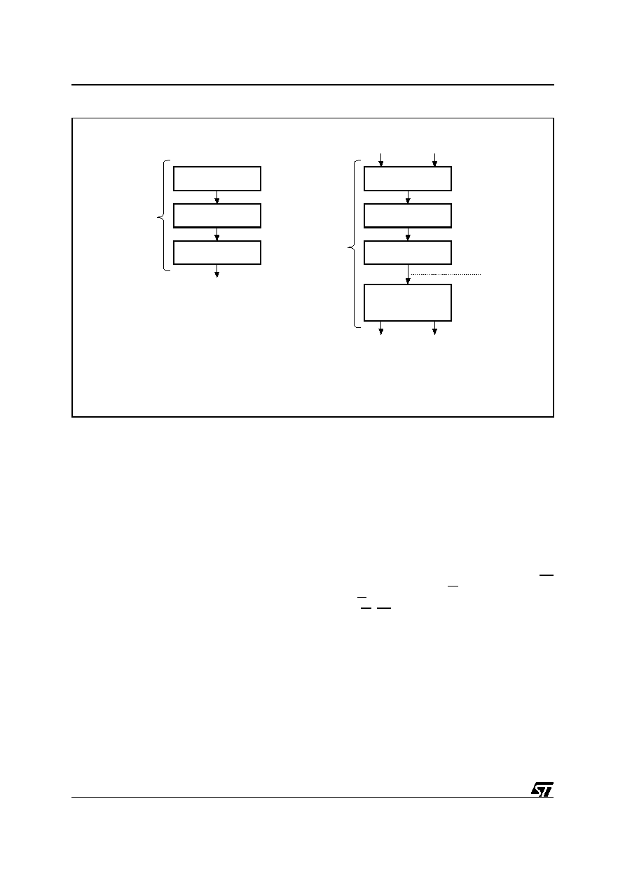
AI01698B
WRITE AAh in
Address 5555h
WRITE 55h in
Address 2AAAh
WRITE A0h in
Address 5555h
SDP is set
WRITE AAh in
Address 5555h
WRITE 55h in
Address 2AAAh
WRITE A0h in
Address 5555h
WRITE Data to
be Written in
any Address
SDP ENABLE ALGORITHM
Page
Write
Instruction
Page
Write
Instruction
WRITE
is enabled
SDP
Set
SDP
not Set
Write
in Memory
Write Data
+
SDP Set
after tWC
Figure 4. EEPROM SDP Enable Flowcharts
8/30
M39208
相关PDF资料 |
PDF描述 |
|---|---|
| M3933/10-17N | 0 MHz - 18000 MHz RF/MICROWAVE FIXED ATTENUATOR |
| M3933/25-65N | 0 MHz - 18000 MHz RF/MICROWAVE FIXED ATTENUATOR |
| M3933/10-16S | 0 MHz - 18000 MHz RF/MICROWAVE FIXED ATTENUATOR |
| M3933/14-23S | 0 MHz - 12400 MHz RF/MICROWAVE FIXED ATTENUATOR |
| M3933/25-31S | 0 MHz - 18000 MHz RF/MICROWAVE FIXED ATTENUATOR |
相关代理商/技术参数 |
参数描述 |
|---|---|
| M39208-15WNB1T | 制造商:STMICROELECTRONICS 制造商全称:STMicroelectronics 功能描述:Single Chip 2 Mbit Flash and 64 Kbit Parallel EEPROM Memory |
| M39208-15WNB5T | 制造商:STMICROELECTRONICS 制造商全称:STMicroelectronics 功能描述:Single Chip 2 Mbit Flash and 64 Kbit Parallel EEPROM Memory |
| M39208-15WNB6T | 制造商:STMICROELECTRONICS 制造商全称:STMicroelectronics 功能描述:Single Chip 2 Mbit Flash and 64 Kbit Parallel EEPROM Memory |
| M39208NA | 制造商:STMICROELECTRONICS 制造商全称:STMicroelectronics 功能描述:Single Chip 2 Mbit Flash and 64 Kbit Parallel EEPROM Memory |
| M39208NB | 制造商:STMICROELECTRONICS 制造商全称:STMicroelectronics 功能描述:Single Chip 2 Mbit Flash and 64 Kbit Parallel EEPROM Memory |
发布紧急采购,3分钟左右您将得到回复。