- 您现在的位置:买卖IC网 > PDF目录299434 > M39208-15WNB1 (STMICROELECTRONICS) 256K X 8 FLASH 2.7V PROM, 150 ns, PDSO32 PDF资料下载
参数资料
| 型号: | M39208-15WNB1 |
| 厂商: | STMICROELECTRONICS |
| 元件分类: | PROM |
| 英文描述: | 256K X 8 FLASH 2.7V PROM, 150 ns, PDSO32 |
| 封装: | 8 X 14 MM, PLASTIC, TSOP-32 |
| 文件页数: | 27/30页 |
| 文件大小: | 218K |
| 代理商: | M39208-15WNB1 |
第1页第2页第3页第4页第5页第6页第7页第8页第9页第10页第11页第12页第13页第14页第15页第16页第17页第18页第19页第20页第21页第22页第23页第24页第25页第26页当前第27页第28页第29页第30页
POWER SUPPLY and CURRENT CONSUMP-
TION
EEPROM Power Down. The M39208 can be set
with the EEPROM in power down with the help of
the EEPROM power down instruction (see Table
4). Once the EEPROM power down instruction is
decoded, the EEPROM block cannot be accessed
unless a further Return instruction is decoded.
Deep Power Down. The M39208 can be set in the
lowest ICC consumption mode with the help of the
Deep Power Down instruction (see Table 4). Once
the instruction is decoded, the device is set in a
sleep mode until a Reset instruction is decoded.
Power Up. The M39208 internal logic is reset upon
a power-up condition to Read memory status. Any
Write operation in EEPROM is inhibited during the
first 5 ms following the power-up.
Either EF, EE or W must be tied to VIH during
Power-up for the maximum security of the data
contents and to remove the possibility of a byte
being written on the first rising edge of EF, EE or
W. Any write cycle initiation is locked when Vcc is
below VLKO.
READ
Read operations and instructions can be used to:
– read the contents of the Memory Array (Flash
block and EEPROM block)
– read the Memory Array (Flash block and
EEPROM block) status and identifiers.
Read data (Flash and EEPROM blocks)
Both Chip Enable EF (or EE) and Output Enable
(G) must be low in order to read the data from the
memory.
Read the Manufacturer Identifier
The manufacturer’s identifier can be read with two
methods: a Read operation or a Read instruction.
Read Operation. The manufacturer’s identifier can
be read with a Read operation with specific logic
levels applied on A0, A1, A6 and the VID level (VID
= 12V + 0.5V) on A9 (see Table 5).
Read Instruction. The manufacturer’s identifier
can also be read with a single instruction composed
of 4 operations: 3 specific Write operations (see
Table 4) and a Read which outputs the Manufac-
turer identifier, the Flash block identifier or the Flash
sector protection status.
Read the Flash Block Identifier
The Flash block identifier can be read with two
methods: a Read operation or a Read instruction.
Read Operation. The Flash block identifier (t.b.d.)
can be read with a single Read operation with
specific logic levels applied on A0, A1, A6 and the
VID level on A9 (see Table 5).
Read Instruction. The Flash block identifier can
also be read with an instruction composed of 4
operations: 3 specific Write operations and a Read
(see Table 4).
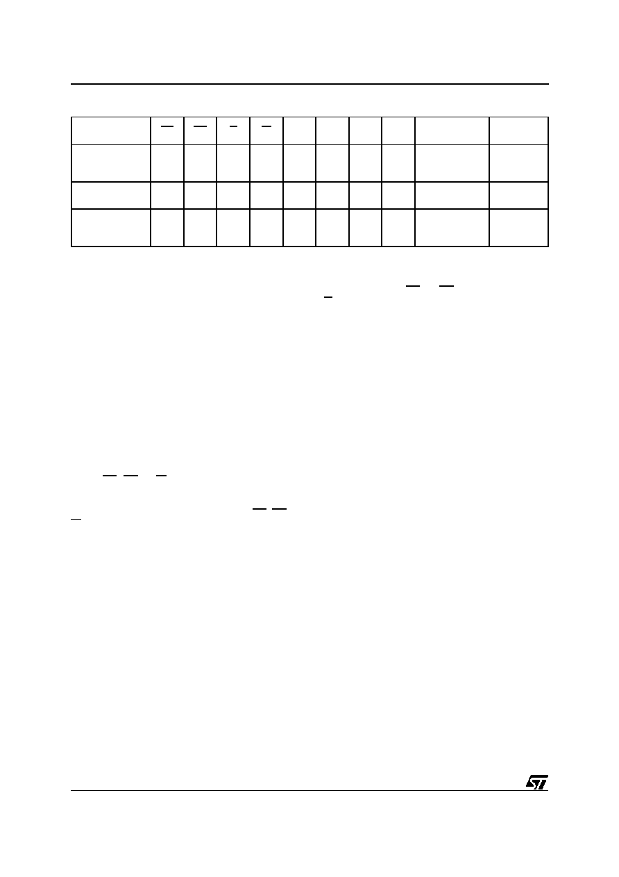
Identifier
EF
EE
G
W
A0A1A6
A9
Other
Addresses
DQ0 - DQ7
Read the
Manufacturer
Identifier
VIL
VIH
VIL
VIH
VIL
VID
Don’t Care
20h
Read the Flash
Block Identifier
VIL
VIH
VIL
VIH
VIL
VID
Don’t Care
t.b.d.
Read the
EEPROM Block
Identifier
VIH
VIL
VIH
XX
VIL
VID
Don’t Care
64 bytes
user
defined
Note: X = Don’t Care.
Table 5. Device Identifiers
6/30
M39208
相关PDF资料 |
PDF描述 |
|---|---|
| M3933/10-17N | 0 MHz - 18000 MHz RF/MICROWAVE FIXED ATTENUATOR |
| M3933/25-65N | 0 MHz - 18000 MHz RF/MICROWAVE FIXED ATTENUATOR |
| M3933/10-16S | 0 MHz - 18000 MHz RF/MICROWAVE FIXED ATTENUATOR |
| M3933/14-23S | 0 MHz - 12400 MHz RF/MICROWAVE FIXED ATTENUATOR |
| M3933/25-31S | 0 MHz - 18000 MHz RF/MICROWAVE FIXED ATTENUATOR |
相关代理商/技术参数 |
参数描述 |
|---|---|
| M39208-15WNB1T | 制造商:STMICROELECTRONICS 制造商全称:STMicroelectronics 功能描述:Single Chip 2 Mbit Flash and 64 Kbit Parallel EEPROM Memory |
| M39208-15WNB5T | 制造商:STMICROELECTRONICS 制造商全称:STMicroelectronics 功能描述:Single Chip 2 Mbit Flash and 64 Kbit Parallel EEPROM Memory |
| M39208-15WNB6T | 制造商:STMICROELECTRONICS 制造商全称:STMicroelectronics 功能描述:Single Chip 2 Mbit Flash and 64 Kbit Parallel EEPROM Memory |
| M39208NA | 制造商:STMICROELECTRONICS 制造商全称:STMicroelectronics 功能描述:Single Chip 2 Mbit Flash and 64 Kbit Parallel EEPROM Memory |
| M39208NB | 制造商:STMICROELECTRONICS 制造商全称:STMicroelectronics 功能描述:Single Chip 2 Mbit Flash and 64 Kbit Parallel EEPROM Memory |
发布紧急采购,3分钟左右您将得到回复。