- 您现在的位置:买卖IC网 > PDF目录296386 > M392T5160CJA-CCC 512M X 72 DDR DRAM MODULE, 0.6 ns, DMA240 PDF资料下载
参数资料
| 型号: | M392T5160CJA-CCC |
| 元件分类: | DRAM |
| 英文描述: | 512M X 72 DDR DRAM MODULE, 0.6 ns, DMA240 |
| 封装: | DIMM-240 |
| 文件页数: | 15/30页 |
| 文件大小: | 718K |
| 代理商: | M392T5160CJA-CCC |
第1页第2页第3页第4页第5页第6页第7页第8页第9页第10页第11页第12页第13页第14页当前第15页第16页第17页第18页第19页第20页第21页第22页第23页第24页第25页第26页第27页第28页第29页第30页
Rev. 1.3 July 2007
RDIMM
DDR2 SDRAM
22 of 30
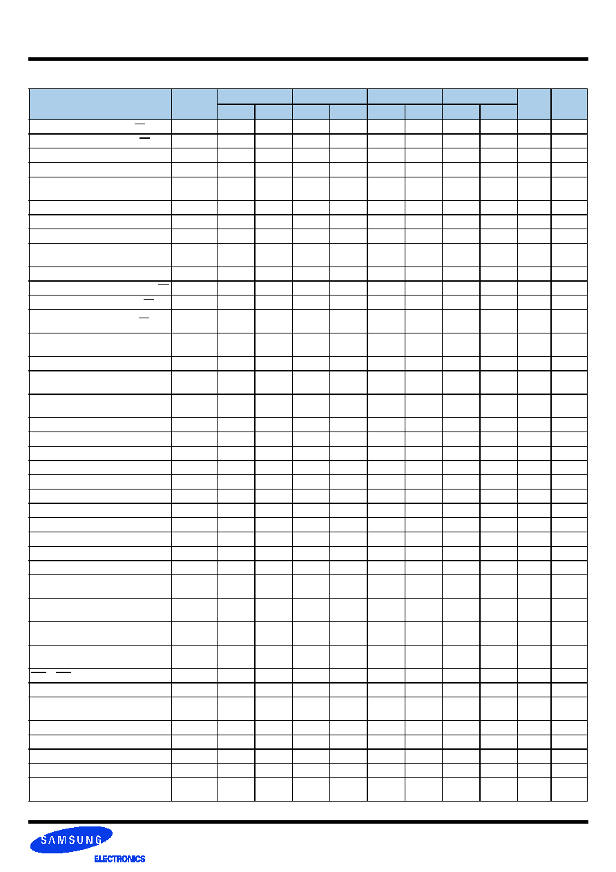
Parameter
Symbol
DDR2-800
DDR2-667
DDR2-533
DDR2-400
Units
Notes
min
max
min
max
min
max
min
max
DQ output access time from CK/CK
tAC
- 400
400
-450
+450
-500
+500
-600
+600
ps
DQS output access time from CK/CK
tDQSCK
- 350
350
-400
+400
-450
+450
-500
+500
ps
CK high-level width
tCH
0.45
0.55
0.45
0.55
0.45
0.55
0.45
0.55
tCK
CK low-level width
tCL
0.45
0.55
0.45
0.55
0.45
0.55
0.45
0.55
tCK
CK half period
tHP
min(tCL,t
CH)
x
min(tCL,
tCH)
x
min(tCL,
tCH)
x
min(tCL,
tCH)
x
ps
Clock cycle time, CL=x
tCK
2500
8000
3000
8000
3750
8000
5000
8000
ps
DQ and DM input hold time
tDH(base)
125
x
175
x
225
x275
x
ps
DQ and DM input setup time
tDS(base)
50
x
100
x
100
x150
x
ps
Control & Address input pulse width for
each input
tIPW
0.6
x
0.6
x
0.6
x0.6
x
tCK
DQ and DM input pulse width for each input tDIPW
0.35
x
0.35
x
0.35
x0.35
x
tCK
Data-out high-impedance time from CK/CK tHZ
x
tAC max
x
tAC max
x
tAC max
x
tAC max
ps
DQS low-impedance time from CK/CK
tLZ(DQS)
tAC min
tAC max
tAC min
tAC max
tAC min
tAC max
tAC min
tAC max
ps
DQ low-impedance time from CK/CK
tLZ(DQ)
2* tAC
min
tAC max
2*tAC
min
tAC max 2* tACmin tAC max 2* tACmin
tAC max
ps
DQS-DQ skew for DQS and associated DQ
signals
tDQSQ
x
200
x
240
x
300
x
350
ps
DQ hold skew factor
tQHS
x
300
x
340
x
400
x
450
ps
DQ/DQS output hold time from DQS
tQH
tHP -
tQHS
x
tHP -
tQHS
x
tHP -
tQHS
x
tHP -
tQHS
x
ps
First DQS latching transition to associated
clock edge
tDQSS
- 0.25
0.25
-0.25
0.25
-0.25
0.25
-0.25
0.25
tCK
DQS input high pulse width
tDQSH
0.35
x
0.35
x
0.35
x
0.35
x
tCK
DQS input low pulse width
tDQSL
0.35
x
0.35
x
0.35
x
0.35
x
tCK
DQS falling edge to CK setup time
tDSS
0.2
x
0.2
x
0.2
x
0.2
x
tCK
DQS falling edge hold time from CK
tDSH
0.2
x
0.2
x
0.2
x
0.2
x
tCK
Mode register set command cycle time
tMRD
2
x
2
x
2
x
2
x
tCK
Write postamble
tWPST
0.4
0.6
0.4
0.6
0.4
0.6
0.4
0.6
tCK
Write preamble
tWPRE
0.35
x
0.35
x
0.35
x
0.35
x
tCK
Address and control input hold time
tIH(base)
250
x
275
x375
x
475
x
ps
Address and control input setup time
tIS(base)
175
x
200
x250
x
350
x
ps
Read preamble
tRPRE
0.9
1.1
0.9
1.1
0.9
1.1
0.9
1.1
tCK
Read postamble
tRPST
0.4
0.6
0.4
0.6
0.4
0.6
0.4
0.6
tCK
Active to active command period for 1KB
page size products
tRRD
7.5
x
7.5
x7.5
x
7.5
x
ns
Active to active command period for 2KB
page size products
tRRD
10
x
10
x10
x
10
x
ns
Four Activate Window for 1KB page size
products
tFAW
35
37.5
ns
Four Activate Window for 2KB page size
products
tFAW
45
50
ns
CAS to CAS command delay
tCCD
2
x
2
tCK
Write recovery time
tWR
15
x
15
x15
x
15
x
ns
Auto precharge write recovery + precharge
time
tDAL
WR+tRP
x
WR+tRP
x
WR+tRP
x
WR+tRP
x
tCK
Internal write to read command delay
tWTR
7.5
x7.5
x10
x
ns
Internal read to precharge command delay tRTP
7.5
ns
Exit self refresh to a non-read command
tXSNR
tRFC + 10
ns
Exit self refresh to a read command
tXSRD
200
x
200
tCK
Exit precharge power down to any non-
read command
tXP
2
x
2
x
2
x
2
x
tCK
13.3 Timing Parameters by Speed Grade
相关PDF资料 |
PDF描述 |
|---|---|
| M3933/14-02N | 0 MHz - 12400 MHz RF/MICROWAVE FIXED ATTENUATOR |
| MIL-A-3933/14-02 | 0 MHz - 12400 MHz RF/MICROWAVE FIXED ATTENUATOR |
| MIL-A-3933/14-14 | 0 MHz - 12400 MHz RF/MICROWAVE FIXED ATTENUATOR |
| M3933/14-18S | 0 MHz - 12400 MHz RF/MICROWAVE FIXED ATTENUATOR |
| MIL-A-3933/14-17 | 0 MHz - 12400 MHz RF/MICROWAVE FIXED ATTENUATOR |
相关代理商/技术参数 |
参数描述 |
|---|---|
| M392T5160CJA-CF7 | 制造商:SAMSUNG 制造商全称:Samsung semiconductor 功能描述:DDR2 Registered SDRAM MODULE |
| M392T5160QJMA | 制造商:SAMSUNG 制造商全称:Samsung semiconductor 功能描述:DDR2 SDRAM Memory |
| M392T5660FBA | 制造商:SAMSUNG 制造商全称:Samsung semiconductor 功能描述:DDR2 SDRAM Memory |
| M392T5660QZHA | 制造商:SAMSUNG 制造商全称:Samsung semiconductor 功能描述:DDR2 SDRAM Memory |
| M392T5663FBA | 制造商:SAMSUNG 制造商全称:Samsung semiconductor 功能描述:DDR2 SDRAM Memory |
发布紧急采购,3分钟左右您将得到回复。