- 您现在的位置:买卖IC网 > PDF目录296386 > M392T5160CJA-CCC 512M X 72 DDR DRAM MODULE, 0.6 ns, DMA240 PDF资料下载
参数资料
| 型号: | M392T5160CJA-CCC |
| 元件分类: | DRAM |
| 英文描述: | 512M X 72 DDR DRAM MODULE, 0.6 ns, DMA240 |
| 封装: | DIMM-240 |
| 文件页数: | 27/30页 |
| 文件大小: | 718K |
| 代理商: | M392T5160CJA-CCC |
第1页第2页第3页第4页第5页第6页第7页第8页第9页第10页第11页第12页第13页第14页第15页第16页第17页第18页第19页第20页第21页第22页第23页第24页第25页第26页当前第27页第28页第29页第30页
Rev. 1.3 July 2007
RDIMM
DDR2 SDRAM
6 of 30
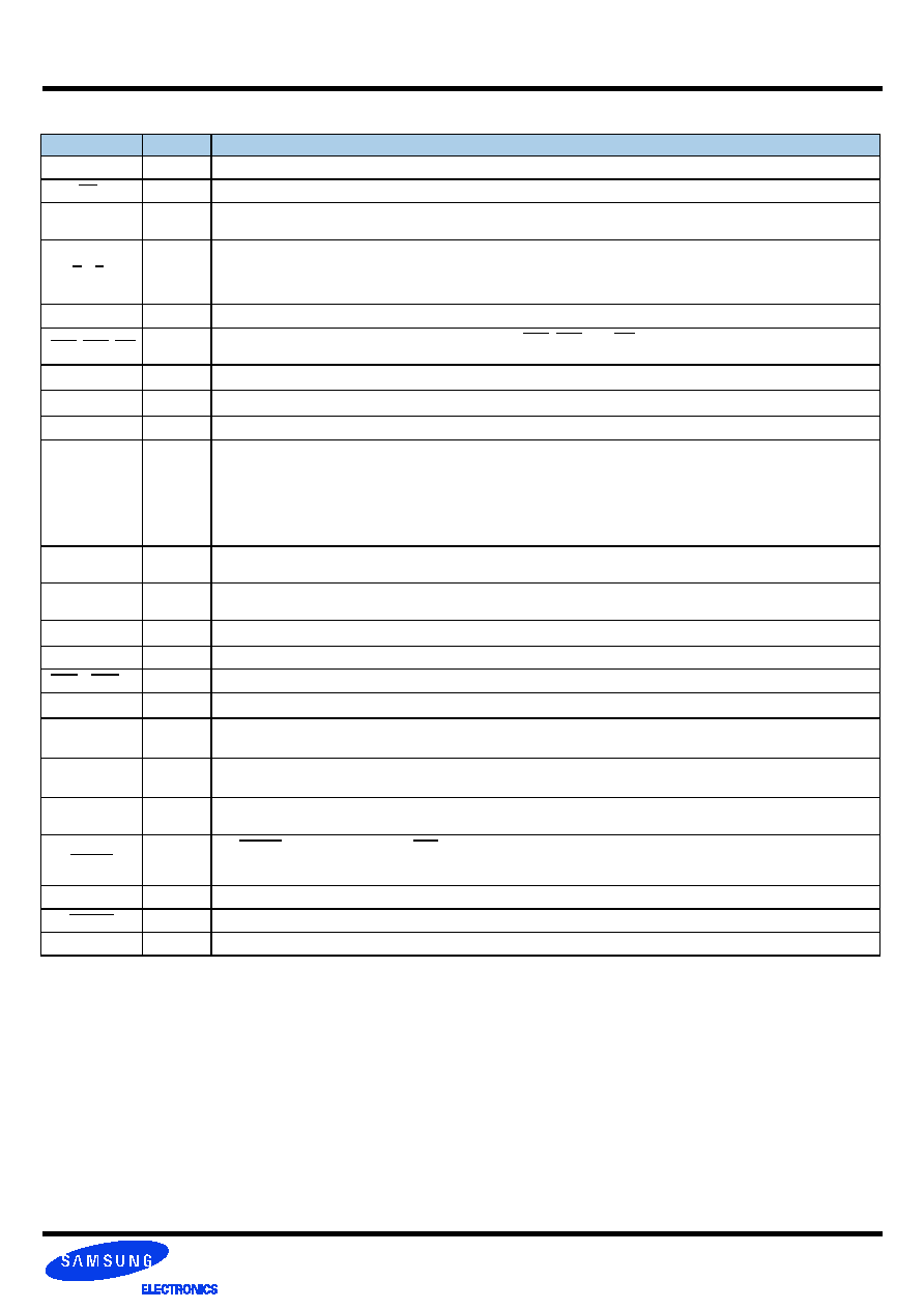
Symbol
Type
Description
CK0
Input
Positive line of the differential pair of system clock inputs that drives input to the on-DIMM PLL.
CK0
Input
Negative line of the differential pair of system clock inputs that drives the input to the on-DIMM PLL.
CKE0~CKE1
Input
Activates the SDRAM CK signal when high and deactivates the CK signal when low. By deactivating the clocks, CKE low
initiates the Power Down mode, or the Self Refresh mode.
S0~S3
Input
Enables the associated SDRAM command decoder when low and disables decoder when high. When decoder is dis-
abled, new commands are ignored but previous operations continue.
These input signals also disable all outputs (except CKE and ODT) of the register(s) on the DIMM when both inputs are
high.
ODT0~ODT1
Input
I/O bus impedance control signals.
RAS, CAS, WE
Input
When sampled at the positive rising edge of the clock, CAS, RAS, and WE define the operation to be executed by the
SDRAM.
VREF
Supply
Reference voltage for SSTL_18 inputs
VDDQ
Supply
Isolated power supply for the DDR SDRAM output buffers to provide improved noise immunity
BA0~BA2
Input
Selects which SDRAM bank of eight is activated.
A0~A9,A10/AP
A11~A13
Input
During a Bank Activate command cycle, Address defines the row address.
During a Read or Write command cycle, Address defines the column address. In addition to the column address, AP is
used to invoke autoprecharge operation at the end of the burst read or write cycle. If AP is high, autoprecharge is selected
and BA0, BA1, BA2 defines the bank to be precharged. If AP is low, autoprecharge is disabled. During a Precharge com-
mand cycle, AP is used in conjunction with BA0, BA1, BA2 to control which bank(s) to precharge. If AP is high, all banks
will be precharged regardless of the state of BA0 or BA1 or BA2. If AP is low, BA0 and BA1 and BA2 are used to define
which bank to precharge.
DQ0~63,
CB0~CB7
In/Out
Data and Check Bit Input/Output pins
DM0~DM8
Input
Masks write data when high, issued concurrently with input data. Both DM and DQ have a write latency of one clock once
the write command is registered into the SDRAM.
VDD, VSS
Supply
Power and ground for the DDR SDRAM input buffers and core logic
DQS0~DQS17
In/Out
Positive line of the differential data strobe for input and output data.
DQS0~DQS17
In/Out
Negative line of the differential data strobe for input and output data.
SA0~SA2
Input
These signals are tied at the system planar to either VSS or VDDSPD to configure the serial SPD EEPROM address range.
SDA
In/Out
This bidirectional pin is used to transfer data into or out of the SPD EEPROM. A resistor must be connected from the SDA
bus line to VDDSPD to act as a pullup.
SCL
Input
This signal is used to clock data into and out of the SPD EEPROM. A resistor may be connected from the SCL bus time
to VDDSPD to act as a pullup.
VDDSPD
Supply
Serial EEPROM positive power supply (wired to a separate power pin at the connector which supports from 1.7 Volt to 3.6
Volt operation).
RESET
Input
The RESET pin is connected to the RST pin on the register and to the OE pin on the PLL. When low, all register outputs
will be driven low and the PLL clocks to the DRAMs and register(s) will be set to low level (The PLL will remain synchro-
nized with the input clock )
Par_In
Input
Parity bit for the Address and Control bus. ( “1 “ : Odd, “0 “ : Even)
Err_Out
Output
Parity error found in the Address and Control bus
TEST
In/Out
Used by memory bus analysis tools (unused on memory DIMMs)
6.0 Input/Output Function Description
相关PDF资料 |
PDF描述 |
|---|---|
| M3933/14-02N | 0 MHz - 12400 MHz RF/MICROWAVE FIXED ATTENUATOR |
| MIL-A-3933/14-02 | 0 MHz - 12400 MHz RF/MICROWAVE FIXED ATTENUATOR |
| MIL-A-3933/14-14 | 0 MHz - 12400 MHz RF/MICROWAVE FIXED ATTENUATOR |
| M3933/14-18S | 0 MHz - 12400 MHz RF/MICROWAVE FIXED ATTENUATOR |
| MIL-A-3933/14-17 | 0 MHz - 12400 MHz RF/MICROWAVE FIXED ATTENUATOR |
相关代理商/技术参数 |
参数描述 |
|---|---|
| M392T5160CJA-CF7 | 制造商:SAMSUNG 制造商全称:Samsung semiconductor 功能描述:DDR2 Registered SDRAM MODULE |
| M392T5160QJMA | 制造商:SAMSUNG 制造商全称:Samsung semiconductor 功能描述:DDR2 SDRAM Memory |
| M392T5660FBA | 制造商:SAMSUNG 制造商全称:Samsung semiconductor 功能描述:DDR2 SDRAM Memory |
| M392T5660QZHA | 制造商:SAMSUNG 制造商全称:Samsung semiconductor 功能描述:DDR2 SDRAM Memory |
| M392T5663FBA | 制造商:SAMSUNG 制造商全称:Samsung semiconductor 功能描述:DDR2 SDRAM Memory |
发布紧急采购,3分钟左右您将得到回复。