- 您现在的位置:买卖IC网 > PDF目录9966 > MAX1038AEEE+T (Maxim Integrated Products)IC ADC 8BIT LP SERIAL 16-QSOP PDF资料下载
参数资料
| 型号: | MAX1038AEEE+T |
| 厂商: | Maxim Integrated Products |
| 文件页数: | 4/23页 |
| 文件大小: | 0K |
| 描述: | IC ADC 8BIT LP SERIAL 16-QSOP |
| 产品培训模块: | Lead (SnPb) Finish for COTS Obsolescence Mitigation Program |
| 标准包装: | 2,500 |
| 位数: | 8 |
| 采样率(每秒): | 188k |
| 数据接口: | I²C,串行 |
| 转换器数目: | 1 |
| 功率耗散(最大): | 1.75mW |
| 电压电源: | 单电源 |
| 工作温度: | -40°C ~ 85°C |
| 安装类型: | 表面贴装 |
| 封装/外壳: | 16-SSOP(0.154",3.90mm 宽) |
| 供应商设备封装: | 16-QSOP |
| 包装: | 带卷 (TR) |
| 输入数目和类型: | 12 个单端,单极;12 个单端,双极;6 个伪差分,单极;6 个伪差分,双极 |
MAX1036–MAX1039
SCL is high (Figure 5). A repeated START condition (Sr)
can be used in place of a STOP condition to leave the
bus active and in its current timing mode (see the
HS-
Mode section).
Acknowledge Bits
Successful data transfers are acknowledged with an
acknowledge bit (A) or a not-acknowledge bit (A). Both
the master and the MAX1036–MAX1039 (slave) generate
acknowledge bits. To generate an “acknowledge,” the
receiving device must pull SDA low before the rising
edge of the acknowledge related clock pulse (ninth
pulse) and keep it low during the high period of the clock
pulse (Figure 6). To generate a “not acknowledge,” the
receiver allows SDA to be pulled high before the rising
edge of the acknowledge related clock pulse and leaves
it high during the high period of the clock pulse.
Monitoring the acknowledge bits allows for detection of
unsuccessful data transfers. An unsuccessful data
transfer happens if a receiving device is busy or if a
system fault has occurred. In the event of an unsuc-
cessful data transfer, the bus master should reattempt
communication at a later time.
Slave Address
A bus master initiates communication with a slave
device by issuing a START condition followed by a
slave address. When idle, the MAX1036–MAX1039 con-
tinuously wait for a START condition followed by their
slave address. When the MAX1036–MAX1039 recog-
nize their slave address, they are ready to accept or
send data. The slave address has been factory pro-
grammed and is always 1100100 for the MAX1036/
MAX1037, and 1100101 for MAX1038/ MAX1039
(Figure 7). The least significant bit (LSB) of the address
byte (R/W) determines whether the master is writing to
or reading from the MAX1036–MAX1039 (R/W = zero
selects a write condition. R/W = 1 selects a read condi-
tion). After receiving the address, the MAX1036–
MAX1039 (slave) issue an acknowledge by pulling SDA
low for one clock cycle.
Bus Timing
At power-up, the MAX1036–MAX1039 bus timing
defaults to fast mode (F/S-mode) allowing conversion
rates up to 44ksps. The MAX1036–MAX1039 must
operate in high-speed mode (HS-mode) to achieve
conversion rates up to 188ksps. Figure 1 shows the bus
timing for the MAX1036–MAX1039’s 2-wire interface.
HS-Mode
At power-up, the MAX1036–MAX1039 bus timing is set
for F/S-mode. The master selects HS-mode by address-
ing all devices on the bus with the HS-mode master
code 0000 1XXX (X = Don’t care). After successfully
receiving the HS-mode master code, the MAX1036–
MAX1039 issues a not acknowledge, allowing SDA to be
pulled high for one clock cycle (Figure 8). After the not
acknowledge, the MAX1036–MAX1039 are in HS-mode.
The master must then send a repeated START followed
by a slave address to initiate HS-mode communication. If
the master generates a STOP condition, the
MAX1036–MAX1039 return to F/S-mode.
Configuration/Setup Bytes (Write Cycle)
Write cycles begin with the master issuing a START
condition followed by 7 address bits (Figure 7) and 1
write bit (R/W = zero). If the address byte is successful-
ly received, the MAX1036–MAX1039 (slave) issue an
acknowledge. The master then writes to the slave. The
slave recognizes the received byte as the setup byte
(Table 1) if the most significant bit (MSB) is 1. If the
MSB is zero, the slave recognizes that byte as the con-
figuration byte (Table 2). The master can write either 1
or 2 bytes to the slave in any order (setup byte then
configuration byte; configuration byte then setup byte;
setup byte only; configuration byte only; Figure 9). If the
slave receives bytes successfully, it issues an acknowl-
edge. The master ends the write cycle by issuing a
STOP condition or a repeated START condition. When
operating in HS-mode, a STOP condition returns the
bus to F/S-mode (see the
HS-Mode section).
Data Byte (Read Cycle)
A read cycle must be initiated to obtain conversion
results. Read cycles begin with the bus master issuing
2.7V to 3.6V and 4.5V to 5.5V, Low-Power,
4-/12-Channel 2-Wire Serial 8-Bit ADCs
12
______________________________________________________________________________________
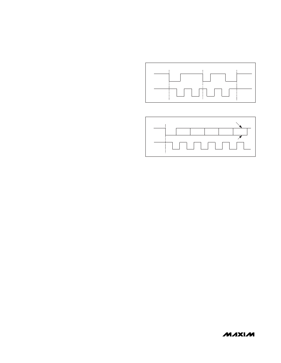
SCL
SDA
SP
Sr
Figure 5. START and STOP Conditions
SCL
SDA
S
NOT ACKNOWLEDGE
ACKNOWLEDGE
12
8
9
Figure 6. Acknowledge Bits
相关PDF资料 |
PDF描述 |
|---|---|
| IDT72845LB15PFI | IC FIFO SYNC DL 4096X18 128TQFP |
| VI-211-MX-F1 | CONVERTER MOD DC/DC 12V 75W |
| VI-B3Z-MX | CONVERTER MOD DC/DC 2V 30W |
| HIN202CBNZ-T | IC 2DRVR/2RCVR RS232 5V 16-SOIC |
| VI-21K-MX-F3 | CONVERTER MOD DC/DC 40V 75W |
相关代理商/技术参数 |
参数描述 |
|---|---|
| MAX1038EVKIT | 功能描述:数据转换 IC 开发工具 RoHS:否 制造商:Texas Instruments 产品:Demonstration Kits 类型:ADC 工具用于评估:ADS130E08 接口类型:SPI 工作电源电压:- 6 V to + 6 V |
| MAX1038KAEEE | 功能描述:模数转换器 - ADC RoHS:否 制造商:Texas Instruments 通道数量:2 结构:Sigma-Delta 转换速率:125 SPs to 8 KSPs 分辨率:24 bit 输入类型:Differential 信噪比:107 dB 接口类型:SPI 工作电源电压:1.7 V to 3.6 V, 2.7 V to 5.25 V 最大工作温度:+ 85 C 安装风格:SMD/SMT 封装 / 箱体:VQFN-32 |
| MAX1038LAEEE | 功能描述:模数转换器 - ADC RoHS:否 制造商:Texas Instruments 通道数量:2 结构:Sigma-Delta 转换速率:125 SPs to 8 KSPs 分辨率:24 bit 输入类型:Differential 信噪比:107 dB 接口类型:SPI 工作电源电压:1.7 V to 3.6 V, 2.7 V to 5.25 V 最大工作温度:+ 85 C 安装风格:SMD/SMT 封装 / 箱体:VQFN-32 |
| MAX1038MAEEE | 功能描述:模数转换器 - ADC RoHS:否 制造商:Texas Instruments 通道数量:2 结构:Sigma-Delta 转换速率:125 SPs to 8 KSPs 分辨率:24 bit 输入类型:Differential 信噪比:107 dB 接口类型:SPI 工作电源电压:1.7 V to 3.6 V, 2.7 V to 5.25 V 最大工作温度:+ 85 C 安装风格:SMD/SMT 封装 / 箱体:VQFN-32 |
| MAX1039 | 制造商:MAXIM 制造商全称:Maxim Integrated Products 功能描述:2.7V to 5.5V, Low-Power, 4-/12-Channel 2-Wire Serial 8-Bit ADCs |
发布紧急采购,3分钟左右您将得到回复。