- 您现在的位置:买卖IC网 > PDF目录2008 > MAX1183ECM+TD (Maxim Integrated Products)IC ADC 10BIT 40MSPS DL 48-TQFP PDF资料下载
参数资料
| 型号: | MAX1183ECM+TD |
| 厂商: | Maxim Integrated Products |
| 文件页数: | 3/18页 |
| 文件大小: | 0K |
| 描述: | IC ADC 10BIT 40MSPS DL 48-TQFP |
| 产品培训模块: | Lead (SnPb) Finish for COTS Obsolescence Mitigation Program |
| 标准包装: | 2,000 |
| 位数: | 10 |
| 采样率(每秒): | 40M |
| 数据接口: | 并联 |
| 转换器数目: | 2 |
| 功率耗散(最大): | 180mW |
| 电压电源: | 单电源 |
| 工作温度: | -40°C ~ 85°C |
| 安装类型: | 表面贴装 |
| 封装/外壳: | 48-TQFP 裸露焊盘 |
| 供应商设备封装: | 48-TQFP 裸露焊盘(7x7) |
| 包装: | 带卷 (TR) |
| 输入数目和类型: | 4 个单端,双极;2 个差分,双极 |
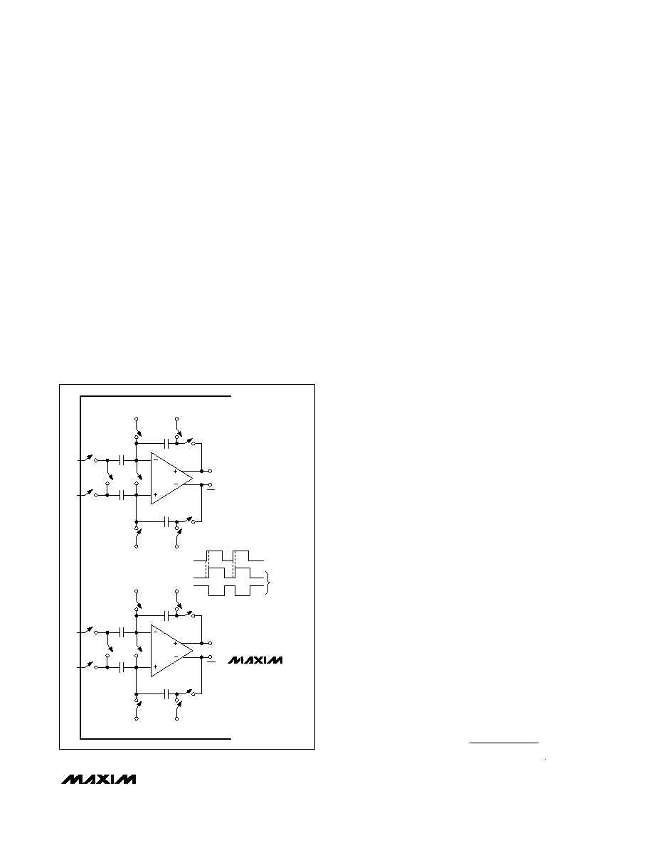
Input Track-and-Hold (T/H) Circuits
Figure 2 displays a simplified functional diagram of the
input track-and-hold (T/H) circuits in both track-and-hold
mode. In track mode, switches S1, S2a, S2b, S4a, S4b,
S5a, and S5b are closed. The fully differential circuits
sample the input signals onto the two capacitors (C2a
and C2b) through switches S4a and S4b. S2a and S2b
set the common mode for the amplifier input, and open
simultaneously with S1, sampling the input waveform.
Switches S4a and S4b are then opened before switch-
es S3a and S3b connect capacitors C1a and C1b to
the output of the amplifier and switch S4c is closed.
The resulting differential voltages are held on capaci-
tors C2a and C2b. The amplifiers are used to charge
capacitors C1a and C1b to the same values originally
held on C2a and C2b. These values are then presented
to the first-stage quantizers and isolate the pipelines
from the fast-changing inputs. The wide input bandwidth
T/H amplifiers allow the MAX1183 to track-and-sam-
ple/hold analog inputs of high frequencies (> Nyquist).
The ADC inputs (INA+, INB+, INA- and INB-) can be
driven either differentially or single-ended. Match the
impedance of INA+ and INA-, as well as INB+ and INB-
and set the common-mode voltage to midsupply
(VDD/2) for optimum performance.
Analog Inputs and Reference
Configurations
The full-scale range of the MAX1183 is determined by
the internally generated voltage difference between
REFP (VDD/2 + VREFIN/4) and REFN (VDD/2 -
VREFIN/4). The full-scale range for both on-chip ADCs is
adjustable through the REFIN pin, which is provided for
this purpose. REFOUT, REFP, COM (VDD/2), and REFN
are internally buffered low-impedance outputs.
The MAX1183 provides three modes of reference
operation:
Internal reference mode
Buffered external reference mode
Unbuffered external reference mode
In internal reference mode, connect the internal refer-
ence output REFOUT to REFIN through a resistor (e.g.,
10k) or resistor divider, if an application requires a
reduced full-scale range. For stability and noise filtering
purposes, bypass REFIN with a >10nF capacitor to
GND. In internal reference mode, REFOUT, COM, REFP,
and REFN become low-impedance outputs.
In buffered external reference mode, adjust the reference
voltage levels externally by applying a stable and accu-
rate voltage at REFIN. In this mode, COM, REFP, and
REFN become outputs. REFOUT may be left open or
connected to REFIN through a >10k resistor.
In unbuffered external reference mode, connect REFIN
to GND. This deactivates the on-chip reference buffers
for REFP, COM, and REFN. With their buffers shut
down, these nodes become high impedance and may
be driven through separate external reference sources.
Clock Input (CLK)
The MAX1183’s CLK input accepts CMOS-compatible
clock signals. Since the interstage conversion of the
device depends on the repeatability of the rising and
falling edges of the external clock, use a clock with low
jitter and fast rise and fall times (< 2ns). In particular,
sampling occurs on the rising edge of the clock signal,
requiring this edge to provide lowest possible jitter. Any
significant aperture jitter would limit the SNR perfor-
mance of the on-chip ADCs as follows:
MAX1183
Dual 10-Bit, 40Msps, 3V, Low-Power ADC with
Internal Reference and Parallel Outputs
______________________________________________________________________________________
11
S3b
S3a
COM
S5b
S5a
INB+
INB-
S1
OUT
C2a
C2b
S4c
S4a
S4b
C1b
C1a
INTERNAL
BIAS
INTERNAL
BIAS
COM
HOLD
CLK
INTERNAL
NONOVERLAPPING
CLOCK SIGNALS
TRACK
S2a
S2b
S3b
S3a
COM
S5b
S5a
INA+
INA-
S1
OUT
C2a
C2b
S4c
S4a
S4b
C1b
C1a
INTERNAL
BIAS
INTERNAL
BIAS
COM
S2a
S2b
MAX1183
Figure 2. MAX1183 T/H Amplifiers
SNR
ft
IN
AJ
log
=×
××
×
20
1
2
π
相关PDF资料 |
PDF描述 |
|---|---|
| MAX1184ECM+TD | IC ADC 10BIT 20MSPS DL 48-TQFP |
| MAX1186ECM+TD | IC ADC 10BIT 40MSPS DL 48-TQFP |
| MAX1187CCUI+ | IC ADC 16BIT 135KSPS 28-TSSOP |
| MAX118EAI+ | IC ADC 8BIT 1MSPS 28-SSOP |
| MAX1191ETI+T | IC ADC 8BIT 7.5MSPS DL 28-TQFN |
相关代理商/技术参数 |
参数描述 |
|---|---|
| MAX1184ECM | 制造商:Maxim Integrated Products 功能描述:DUAL 10-BIT, 20MSPS, +3V, LOW-POWER ADC WITH - Rail/Tube |
| MAX1184ECM+D | 功能描述:模数转换器 - ADC 10-Bit 2Ch 30Msps High Speed ADC RoHS:否 制造商:Texas Instruments 通道数量:2 结构:Sigma-Delta 转换速率:125 SPs to 8 KSPs 分辨率:24 bit 输入类型:Differential 信噪比:107 dB 接口类型:SPI 工作电源电压:1.7 V to 3.6 V, 2.7 V to 5.25 V 最大工作温度:+ 85 C 安装风格:SMD/SMT 封装 / 箱体:VQFN-32 |
| MAX1184ECM+TD | 功能描述:模数转换器 - ADC 10-Bit 2Ch 30Msps High Speed ADC RoHS:否 制造商:Texas Instruments 通道数量:2 结构:Sigma-Delta 转换速率:125 SPs to 8 KSPs 分辨率:24 bit 输入类型:Differential 信噪比:107 dB 接口类型:SPI 工作电源电压:1.7 V to 3.6 V, 2.7 V to 5.25 V 最大工作温度:+ 85 C 安装风格:SMD/SMT 封装 / 箱体:VQFN-32 |
| MAX1184ECM-D | 功能描述:模数转换器 - ADC RoHS:否 制造商:Texas Instruments 通道数量:2 结构:Sigma-Delta 转换速率:125 SPs to 8 KSPs 分辨率:24 bit 输入类型:Differential 信噪比:107 dB 接口类型:SPI 工作电源电压:1.7 V to 3.6 V, 2.7 V to 5.25 V 最大工作温度:+ 85 C 安装风格:SMD/SMT 封装 / 箱体:VQFN-32 |
| MAX1184ECM-T | 制造商:Maxim Integrated Products 功能描述:DUAL 10-BIT, 20MSPS, +3V, LOW-POWER ADC WITH - Tape and Reel |
发布紧急采购,3分钟左右您将得到回复。