- 您现在的位置:买卖IC网 > PDF目录2008 > MAX1183ECM+TD (Maxim Integrated Products)IC ADC 10BIT 40MSPS DL 48-TQFP PDF资料下载
参数资料
| 型号: | MAX1183ECM+TD |
| 厂商: | Maxim Integrated Products |
| 文件页数: | 5/18页 |
| 文件大小: | 0K |
| 描述: | IC ADC 10BIT 40MSPS DL 48-TQFP |
| 产品培训模块: | Lead (SnPb) Finish for COTS Obsolescence Mitigation Program |
| 标准包装: | 2,000 |
| 位数: | 10 |
| 采样率(每秒): | 40M |
| 数据接口: | 并联 |
| 转换器数目: | 2 |
| 功率耗散(最大): | 180mW |
| 电压电源: | 单电源 |
| 工作温度: | -40°C ~ 85°C |
| 安装类型: | 表面贴装 |
| 封装/外壳: | 48-TQFP 裸露焊盘 |
| 供应商设备封装: | 48-TQFP 裸露焊盘(7x7) |
| 包装: | 带卷 (TR) |
| 输入数目和类型: | 4 个单端,双极;2 个差分,双极 |
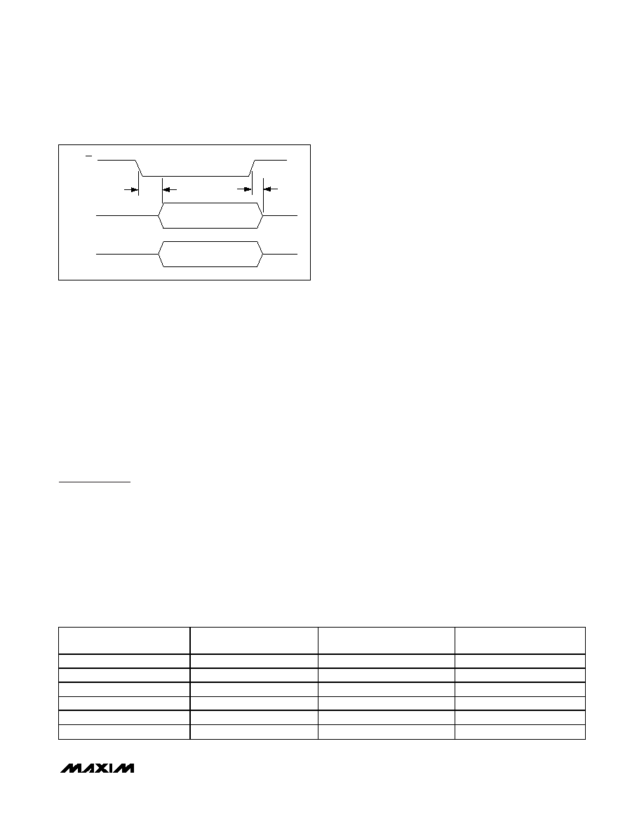
Figure 4 displays the timing relationship between output
enable and data output valid, as well as power-
down/wake-up and data output valid.
Power-Down (PD) and Sleep
(SLEEP) Modes
The MAX1183 offers two power-save modes—sleep and
full power-down modes. In sleep mode (SLEEP = 1), only
the reference bias circuit is active (both ADCs are
disabled), and current consumption is reduced to 2.8mA.
To enter full power-down mode, pull PD high. With
OE
simultaneously low, all outputs are latched at the last
value prior to the power down. Pulling
OE high forces
the digital outputs into a high-impedance state.
Applications Information
Figure 5 depicts a typical application circuit containing
two single-ended to differential converters. The internal
reference provides a VDD/2 output voltage for level-
shifting purposes. The input is buffered and then split
to a voltage follower and inverter. One lowpass filter per
ADC suppresses some of the wideband noise associat-
ed with high-speed op amps follows the amplifiers. The
user may select the RISO and CIN values to optimize
the filter performance, to suit a particular application.
For the application in Figure 5, a RISO of 50 is placed
before the capacitive load to prevent ringing and
oscillation. The 22pF CIN capacitor acts as a small
bypassing capacitor.
Using Transformer Coupling
An RF transformer (Figure 6) provides an excellent solu-
tion to convert a single-ended source signal to a fully dif-
ferential signal, required by the MAX1183 for optimum
performance. Connecting the center tap of the trans-
former to COM provides a VDD/2 DC level shift to the
input. Although a 1:1 transformer is shown, a step-up
transformer may be selected to reduce the drive require-
ments. A reduced signal swing from the input driver, such
as an op amp, may also improve the overall distortion.
In general, the MAX1183 provides better SFDR and
THD with fully differential input signals than single-
ended drive, especially for very high input frequencies.
In differential input mode, even-order harmonics are
lower as both inputs (INA+, INA- and/or INB+, INB-) are
balanced, and each of the ADC inputs only requires
half the signal swing compared to single-ended mode.
Single-Ended AC-Coupled Input Signal
Figure 7 shows an AC-coupled, single-ended applica-
tion. Amplifiers like the MAX4108 provide high speed,
high bandwidth, low noise, and low distortion to main-
tain the integrity of the input signal.
Typical QAM Demodulation Application
The most frequently used modulation technique for dig-
ital communications applications is probably the quad-
rature amplitude modulation (QAM). Typically found in
spread-spectrum-based systems, a QAM signal repre-
sents a carrier frequency modulated in both amplitude
and phase. At the transmitter, modulating the base-
band signal with quadrature outputs, a local oscillator
followed by subsequent up-conversion can generate
the QAM signal. The result is an in-phase (I) and
a quadrature (Q) carrier component, where the Q
MAX1183
Dual 10-Bit, 40Msps, 3V, Low-Power ADC with
Internal Reference and Parallel Outputs
______________________________________________________________________________________
13
OUTPUT
D9A–D0A
OE
tDISABLE
tENABLE
HIGH-Z
VALID DATA
OUTPUT
D9B–D0B
HIGH-Z
VALID DATA
Figure 4. Output Timing Diagram
DIFFERENTIAL INPUT
VOLTAGE*
DIFFERENTIAL INPUT
STRAIGHT OFFSET BINARY
T/B = 0
TWO'S COMPLEMENT
T/B = 1
VREF x 511/512
+FULL SCALE - 1LSB
11 1111 1111
01 1111 1111
VREF x 1/512
+ 1LSB
10 0000 0001
00 0000 0001
0
Bipolar Zero
10 0000 0000
00 0000 0000
- VREF x 1/512
- 1LSB
01 1111 1111
11 1111 1111
-VREF x 512/512
-FULL SCALE +1LSB
00 0000 0001
10 0000 0001
-VREF x 512/512
-FULL SCALE
00 0000 0000
10 0000 0000
Table 1. MAX1183 Output Codes for Differential Inputs
*VREF = VREFP - VREFN
相关PDF资料 |
PDF描述 |
|---|---|
| MAX1184ECM+TD | IC ADC 10BIT 20MSPS DL 48-TQFP |
| MAX1186ECM+TD | IC ADC 10BIT 40MSPS DL 48-TQFP |
| MAX1187CCUI+ | IC ADC 16BIT 135KSPS 28-TSSOP |
| MAX118EAI+ | IC ADC 8BIT 1MSPS 28-SSOP |
| MAX1191ETI+T | IC ADC 8BIT 7.5MSPS DL 28-TQFN |
相关代理商/技术参数 |
参数描述 |
|---|---|
| MAX1184ECM | 制造商:Maxim Integrated Products 功能描述:DUAL 10-BIT, 20MSPS, +3V, LOW-POWER ADC WITH - Rail/Tube |
| MAX1184ECM+D | 功能描述:模数转换器 - ADC 10-Bit 2Ch 30Msps High Speed ADC RoHS:否 制造商:Texas Instruments 通道数量:2 结构:Sigma-Delta 转换速率:125 SPs to 8 KSPs 分辨率:24 bit 输入类型:Differential 信噪比:107 dB 接口类型:SPI 工作电源电压:1.7 V to 3.6 V, 2.7 V to 5.25 V 最大工作温度:+ 85 C 安装风格:SMD/SMT 封装 / 箱体:VQFN-32 |
| MAX1184ECM+TD | 功能描述:模数转换器 - ADC 10-Bit 2Ch 30Msps High Speed ADC RoHS:否 制造商:Texas Instruments 通道数量:2 结构:Sigma-Delta 转换速率:125 SPs to 8 KSPs 分辨率:24 bit 输入类型:Differential 信噪比:107 dB 接口类型:SPI 工作电源电压:1.7 V to 3.6 V, 2.7 V to 5.25 V 最大工作温度:+ 85 C 安装风格:SMD/SMT 封装 / 箱体:VQFN-32 |
| MAX1184ECM-D | 功能描述:模数转换器 - ADC RoHS:否 制造商:Texas Instruments 通道数量:2 结构:Sigma-Delta 转换速率:125 SPs to 8 KSPs 分辨率:24 bit 输入类型:Differential 信噪比:107 dB 接口类型:SPI 工作电源电压:1.7 V to 3.6 V, 2.7 V to 5.25 V 最大工作温度:+ 85 C 安装风格:SMD/SMT 封装 / 箱体:VQFN-32 |
| MAX1184ECM-T | 制造商:Maxim Integrated Products 功能描述:DUAL 10-BIT, 20MSPS, +3V, LOW-POWER ADC WITH - Tape and Reel |
发布紧急采购,3分钟左右您将得到回复。