- 您现在的位置:买卖IC网 > PDF目录2008 > MAX1183ECM+TD (Maxim Integrated Products)IC ADC 10BIT 40MSPS DL 48-TQFP PDF资料下载
参数资料
| 型号: | MAX1183ECM+TD |
| 厂商: | Maxim Integrated Products |
| 文件页数: | 4/18页 |
| 文件大小: | 0K |
| 描述: | IC ADC 10BIT 40MSPS DL 48-TQFP |
| 产品培训模块: | Lead (SnPb) Finish for COTS Obsolescence Mitigation Program |
| 标准包装: | 2,000 |
| 位数: | 10 |
| 采样率(每秒): | 40M |
| 数据接口: | 并联 |
| 转换器数目: | 2 |
| 功率耗散(最大): | 180mW |
| 电压电源: | 单电源 |
| 工作温度: | -40°C ~ 85°C |
| 安装类型: | 表面贴装 |
| 封装/外壳: | 48-TQFP 裸露焊盘 |
| 供应商设备封装: | 48-TQFP 裸露焊盘(7x7) |
| 包装: | 带卷 (TR) |
| 输入数目和类型: | 4 个单端,双极;2 个差分,双极 |
MAX1183
where fIN represents the analog input frequency and
tAJ is the time of the aperture jitter.
Clock jitter is especially critical for undersampling
applications. The clock input should always be consid-
ered as an analog input and routed away from any ana-
log input or other digital signal lines.
The MAX1183 clock input operates with a voltage thresh-
old set to VDD/2. Clock inputs with a duty cycle other
than 50% must meet the specifications for high and low
periods as stated in the Electrical Characteristics.
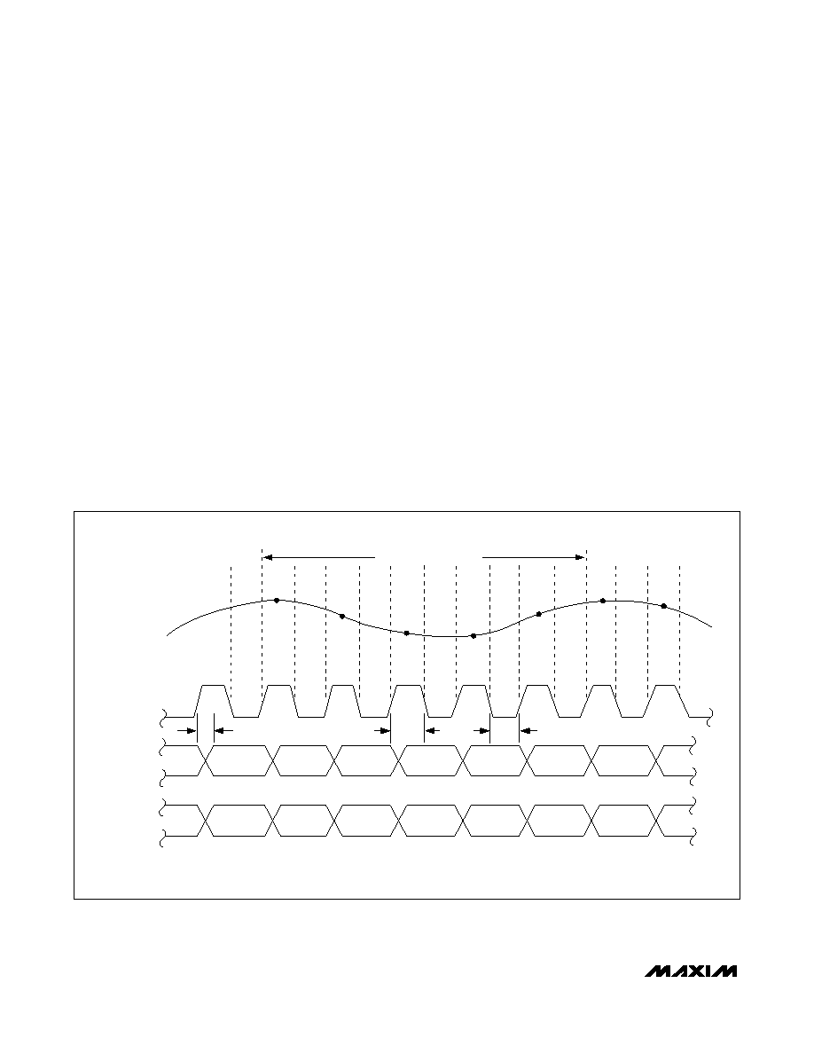
System Timing Requirements
Figure 3 depicts the relationship between the clock
input, analog input, and data output. The MAX1183
samples at the rising edge of the input clock. Output
data for channels A and B is valid on the next rising
edge of the input clock. The output data has an internal
latency of five clock cycles. Figure 4 also determines
the relationship between the input clock parameters
and the valid output data on channels A and B.
Digital Output Data, Output Data Format
Selection (T/B), Output Enable (
OE)
All digital outputs, D0A–D9A (Channel A) and D0B–D9B
(Channel B) are TTL/CMOS logic-compatible. There is a
five-clock-cycle latency between any particular sample
and its corresponding output data. The output coding
can be chosen to be either straight offset binary or
two’s complement (Table 1) controlled by a single pin
(T/B). Pull T/B low to select offset binary and high to
activate two’s complement output coding. The capaci-
tive load on the digital outputs D0A–D9A and D0B–D9B
should be kept as low as possible (<15pF) to avoid
large digital currents that could feed back into the ana-
log portion of the MAX1183, thereby degrading its
dynamic performance. Using buffers on the digital out-
puts of the ADCs can further isolate the digital outputs
from heavy capacitive loads. To further improve the
dynamic performance of the MAX1183, small-series
resistors (e.g., 100) may be added to the digital out-
put paths close to the MAX1183.
Dual 10-Bit, 40Msps, 3V, Low-Power ADC with
Internal Reference and Parallel Outputs
12
______________________________________________________________________________________
N - 6
N
N - 5
N + 1
N - 4
N + 2
N - 3
N + 3
N - 2
N + 4
N - 1
N + 5
N
N + 6
N + 1
5-CLOCK-CYCLE LATENCY
ANALOG INPUT
CLOCK INPUT
DATA OUTPUT
D9A–D0A
tDO
tCH
tCL
N - 6
N - 5
N - 4
N - 3
N - 2
N - 1
N
N + 1
DATA OUTPUT
D9B–D0B
Figure 3. System Timing Diagram
相关PDF资料 |
PDF描述 |
|---|---|
| MAX1184ECM+TD | IC ADC 10BIT 20MSPS DL 48-TQFP |
| MAX1186ECM+TD | IC ADC 10BIT 40MSPS DL 48-TQFP |
| MAX1187CCUI+ | IC ADC 16BIT 135KSPS 28-TSSOP |
| MAX118EAI+ | IC ADC 8BIT 1MSPS 28-SSOP |
| MAX1191ETI+T | IC ADC 8BIT 7.5MSPS DL 28-TQFN |
相关代理商/技术参数 |
参数描述 |
|---|---|
| MAX1184ECM | 制造商:Maxim Integrated Products 功能描述:DUAL 10-BIT, 20MSPS, +3V, LOW-POWER ADC WITH - Rail/Tube |
| MAX1184ECM+D | 功能描述:模数转换器 - ADC 10-Bit 2Ch 30Msps High Speed ADC RoHS:否 制造商:Texas Instruments 通道数量:2 结构:Sigma-Delta 转换速率:125 SPs to 8 KSPs 分辨率:24 bit 输入类型:Differential 信噪比:107 dB 接口类型:SPI 工作电源电压:1.7 V to 3.6 V, 2.7 V to 5.25 V 最大工作温度:+ 85 C 安装风格:SMD/SMT 封装 / 箱体:VQFN-32 |
| MAX1184ECM+TD | 功能描述:模数转换器 - ADC 10-Bit 2Ch 30Msps High Speed ADC RoHS:否 制造商:Texas Instruments 通道数量:2 结构:Sigma-Delta 转换速率:125 SPs to 8 KSPs 分辨率:24 bit 输入类型:Differential 信噪比:107 dB 接口类型:SPI 工作电源电压:1.7 V to 3.6 V, 2.7 V to 5.25 V 最大工作温度:+ 85 C 安装风格:SMD/SMT 封装 / 箱体:VQFN-32 |
| MAX1184ECM-D | 功能描述:模数转换器 - ADC RoHS:否 制造商:Texas Instruments 通道数量:2 结构:Sigma-Delta 转换速率:125 SPs to 8 KSPs 分辨率:24 bit 输入类型:Differential 信噪比:107 dB 接口类型:SPI 工作电源电压:1.7 V to 3.6 V, 2.7 V to 5.25 V 最大工作温度:+ 85 C 安装风格:SMD/SMT 封装 / 箱体:VQFN-32 |
| MAX1184ECM-T | 制造商:Maxim Integrated Products 功能描述:DUAL 10-BIT, 20MSPS, +3V, LOW-POWER ADC WITH - Tape and Reel |
发布紧急采购,3分钟左右您将得到回复。