- 您现在的位置:买卖IC网 > PDF目录9962 > MAX1383ATP+T (Maxim Integrated Products)IC ADC 12BIT 1.25MSPS 20-TQFN PDF资料下载
参数资料
| 型号: | MAX1383ATP+T |
| 厂商: | Maxim Integrated Products |
| 文件页数: | 6/25页 |
| 文件大小: | 0K |
| 描述: | IC ADC 12BIT 1.25MSPS 20-TQFN |
| 产品培训模块: | Lead (SnPb) Finish for COTS Obsolescence Mitigation Program |
| 标准包装: | 2,500 |
| 位数: | 12 |
| 采样率(每秒): | 1.25M |
| 数据接口: | DSP,MICROWIRE?,QSPI?,串行,SPI? |
| 转换器数目: | 2 |
| 功率耗散(最大): | 85.5mW |
| 电压电源: | 单电源 |
| 工作温度: | -40°C ~ 85°C |
| 安装类型: | 表面贴装 |
| 封装/外壳: | 20-WQFN 裸露焊盘 |
| 供应商设备封装: | 20-TQFN-EP(5x5) |
| 包装: | 带卷 (TR) |
| 输入数目和类型: | 2 个单端,单极;2 个单端,双极;1 个差分,单极;1 个差分,双极 |
MAX1377/MAX1379/MAX1383
Dual, 12-Bit, 1.25Msps Simultaneous-Sampling
ADCs with Serial Interface
14
______________________________________________________________________________________
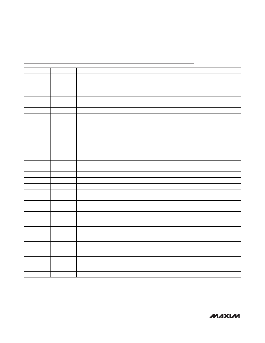
Pin Description
PIN
NAME
FUNCTION
1
REFSEL
Reference-Select Input. Drive REFSEL high to select external reference mode and power down the
internal reference. Drive REFSEL low to select internal reference mode.
2
REF
Internal Reference Output/External Reference Input. For internal reference mode, bypass REF to
RGND with a
≥ 1F capacitor. For external reference mode, apply a reference voltage at REF.
3
RGND
Reference Ground/Common Negative Input. In bipolar mode, RGND is the reference ground. In
unipolar mode, RGND is the common negative input for all four analog inputs (see Figure 3).
4, 18
AGND
Analog Ground
5
AVDD
Analog-Supply Input. Bypass AVDD with a 10F || 10nF capacitor to ground.
6
AIN2A
Primary/Positive Analog Input Channel 2. AIN2A is the primary channel 2 input (AIN2A) if using
single-ended inputs (U/B is low) and the positive channel 2 input (AIN2+) if using differential inputs
(U/B is high) (see Figure 3).
7
AIN2B
Secondary/Negative Analog Input Channel 2. AIN2B is the secondary channel 2 input (AIN2B) if
using single-ended inputs (U/B is low) and the negative channel 2 input (AIN2-) if using differential
inputs (U/B is high) (see Figure 3).
8
U/B
Unipolar/Bipolar Input. Drive U/B low to select unipolar mode. Drive U/B high to select bipolar
mode. In bipolar mode, the analog inputs are differential.
9
DGND
Digital Supply Ground
10
VL
Digital Supply Input. Bypass VL with a 10F || 10nF capacitor to ground.
11
DOUT2
Serial-Data Output 2. Data is clocked out on the rising edge of SCLK.
12
DOUT1
Serial-Data Output 1. Data is clocked out on the rising edge of SCLK.
13
SCLK
Serial-Clock Input. Clocks data out of the serial interface. SCLK also sets the conversion time.
14
CNVST
Conversion-Start Input. Forcing CNVST high prepares the device for a conversion. Conversion
begins on the falling edge of CNVST.
15
CS
Active-Low, Chip-Select Input. Drive CS low to enable the serial interface. When CS is high, DOUT1
and DOUT2 are high impedance, the serial interface resets, and the device powers down.
16
S/D
Single-Output/Dual-Output Selection Input. Drive S/D high to route ADC2 data through DOUT1 after
ADC1 data. Drive S/D low for dual outputs with ADC1 data going to DOUT1 and ADC2 data going
to DOUT2. See the Single-/Dual-Output Modes (S/D) section.
17
SEL
Analog-Input Selection Input. If U/B is low (unipolar mode), drive SEL low to select the primary
inputs, AIN1A and AIN2A. Drive SEL high to select the secondary inputs, AIN1B and AIN2B. In
bipolar mode, SEL is ignored.
19
AIN1B
Secondary/Negative Analog Input Channel 1. AIN1B is the secondary channel 1 input (AIN1B) if
using single-ended inputs (U/B is low) and the negative channel 1 input (AIN1-) if using differential
inputs (U/B is high) (see Figure 3).
20
AIN1A
Primary/Positive Analog Input Channel 1. AIN1A is the primary channel 1 input (AIN1A) if using
single-ended inputs (U/B is low) and the positive channel 1 input (AIN1+) if using differential inputs
(U/B is high) (see Figure 3).
—
EP
Exposed Pad. EP is internally connected to AGND.
相关PDF资料 |
PDF描述 |
|---|---|
| MS27484T20B39PC | CONN PLUG 39POS STRAIGHT W/PINS |
| MS27467T21A41SA | CONN PLUG 41POS STRAIGHT W/SCKT |
| D38999/26FG39PD | CONN PLUG 39POS STRAIGHT W/PINS |
| V48B48M250BG3 | CONVERTER MOD DC/DC 48V 250W |
| D38999/26FG39PC | CONN PLUG 39POS STRAIGHT W/PINS |
相关代理商/技术参数 |
参数描述 |
|---|---|
| MAX1385AETM | 制造商:Maxim Integrated Products 功能描述:12-BIT MULTI-CH ADC WITH MULTICH DA - Rail/Tube |
| MAX1385AETM+ | 制造商:Maxim Integrated Products 功能描述: |
| MAX1385BETM | 制造商:Maxim Integrated Products 功能描述:12-BIT MULTI-CH ADC WITH MULTICH DA - Rail/Tube |
| MAX1385BETM+ | 功能描述:射频放大器 2Ch RF LDMOS Bias Controller RoHS:否 制造商:Skyworks Solutions, Inc. 类型:Low Noise Amplifier 工作频率:2.3 GHz to 2.8 GHz P1dB:18.5 dBm 输出截获点:37.5 dBm 功率增益类型:32 dB 噪声系数:0.85 dB 工作电源电压:5 V 电源电流:125 mA 测试频率:2.6 GHz 最大工作温度:+ 85 C 安装风格:SMD/SMT 封装 / 箱体:QFN-16 封装:Reel |
| MAX1385BETM+T | 功能描述:射频放大器 2Ch RF LDMOS Bias Controller RoHS:否 制造商:Skyworks Solutions, Inc. 类型:Low Noise Amplifier 工作频率:2.3 GHz to 2.8 GHz P1dB:18.5 dBm 输出截获点:37.5 dBm 功率增益类型:32 dB 噪声系数:0.85 dB 工作电源电压:5 V 电源电流:125 mA 测试频率:2.6 GHz 最大工作温度:+ 85 C 安装风格:SMD/SMT 封装 / 箱体:QFN-16 封装:Reel |
发布紧急采购,3分钟左右您将得到回复。