- 您现在的位置:买卖IC网 > PDF目录9962 > MAX1383ATP+T (Maxim Integrated Products)IC ADC 12BIT 1.25MSPS 20-TQFN PDF资料下载
参数资料
| 型号: | MAX1383ATP+T |
| 厂商: | Maxim Integrated Products |
| 文件页数: | 7/25页 |
| 文件大小: | 0K |
| 描述: | IC ADC 12BIT 1.25MSPS 20-TQFN |
| 产品培训模块: | Lead (SnPb) Finish for COTS Obsolescence Mitigation Program |
| 标准包装: | 2,500 |
| 位数: | 12 |
| 采样率(每秒): | 1.25M |
| 数据接口: | DSP,MICROWIRE?,QSPI?,串行,SPI? |
| 转换器数目: | 2 |
| 功率耗散(最大): | 85.5mW |
| 电压电源: | 单电源 |
| 工作温度: | -40°C ~ 85°C |
| 安装类型: | 表面贴装 |
| 封装/外壳: | 20-WQFN 裸露焊盘 |
| 供应商设备封装: | 20-TQFN-EP(5x5) |
| 包装: | 带卷 (TR) |
| 输入数目和类型: | 2 个单端,单极;2 个单端,双极;1 个差分,单极;1 个差分,双极 |
MAX1377/MAX1379/MAX1383
Dual, 12-Bit, 1.25Msps Simultaneous-Sampling
ADCs with Serial Interface
______________________________________________________________________________________
15
Detailed Description
The MAX1377/MAX1379/MAX1383 use an input track
and hold (T/H) and SAR circuitry to convert an analog
input signal to a digital 12-bit output. The dual serial
interface requires a minimum of three digital lines
(SCLK, CNVST, and DOUT) and provides easy interfac-
ing to microprocessors (Ps) and DSPs. Four digital
lines are required for dual-output mode.
Input T/H Circuit
Upon power-up, the input T/H circuit enters its tracking
mode immediately. Following a conversion, the T/H
enters the tracking mode on the 14th SCLK rising edge
of the previous conversion (Figure 6). The T/H enters the
hold mode on the falling edge of CNVST. The time
required for the T/H to acquire an input signal is deter-
mined by how quickly the input capacitance is charged.
If the input signal’s source impedance is high, the acqui-
sition time lengthens. For the MAX1377/MAX1379, the
acquisition time, tACQ, is the minimum time needed for
the signal to be acquired (see the
Definitions section).
tACQ is calculated by the following equation:
tACQ ≥ 9 x (RS + RIN) x CIN (MAX1377/MAX1379)
where RIN = 450, CIN = 16pF, and RS is the source
impedance of the input signal.
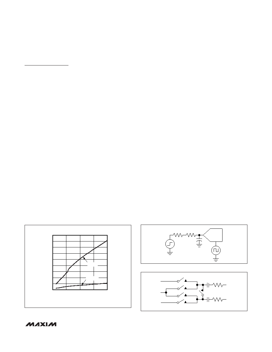
Figure 1 shows the acquisition time as tested using the
circuit of Figure 2. The acquisition time is the time
between the rising edge of a 1V to 3V step input and
the falling edge of CONVST which produced a stable
sample. Rs represents the source impedance of the
function generator (50) and Rx represents the vari-
able filter resistance.
For the MAX1383, tACQ has a typical constant value of
125ns. Also, it has a typical constant input impedance
of 11k. Since the input voltage seen at the pin is a
function of a resistive voltage divider i.e., VIN x RIN/(RIN
+ RX) = VIN x 11k/(11k + RX), it is very important to
select an RX << 11k to avoid large gain error.
MAX1377/MAX1379 Unipolar Mode
The MAX1377/MAX1379 support two simultaneously
sampled, single-ended conversions in unipolar mode.
Drive U/B low for unipolar mode. In unipolar mode,
switches A–D in Figure 3a close according to the posi-
tion of SEL. Drive SEL low to close switches A and D
and designate AIN1A and AIN2A as the active, single-
ended inputs referenced to RGND. Drive SEL high to
close switches B and D and select AIN1B and AIN2B
as the active, single-ended inputs referenced to RGND.
The output code in unipolar mode is straight binary.
See Figure 4a for the unipolar transfer function.
MAX1377/MAX1379 Bipolar Mode
Drive U/B high to configure the inputs for bipolar/differ-
ential mode. Switches A and C in Figure 3a are closed,
designating AIN1A (AIN2A) and AIN1B (AIN2B) as the
active, differential inputs. In bipolar mode, SEL is
ignored. The output code is in two’s complement.
Figure 5 shows the transfer function for bipolar mode.
MAX1383 Input Mode
A ±10V input mode is available on the MAX1383. It is
accomplished by utilizing a resistive divider on the
input followed by a low distortion amplifier to drive the
track and hold circuit. Special high voltage ESD struc-
tures are also utilized on these channels. When using
RGND
A
B
C
D
AIN1A
(AIN2A)
AIN1B
(AIN2B)
CIN
RIN
TO ADC+
TO ADC-
CIN
RIN
Figure 3a. MAX1377/MAX1379 Equivalent Input Circuit
ADC
Rx
Rs
CONVST
C
1V TO 3V
STEP
Figure 2. Test Circuit
MAX1377
fig01
SOURCE IMPEDANCE, Rx ()
ACQUISITION
TIME
(ns)
150
100
50
200
400
600
800
1000
1200
1400
1600
1800
0
0200
C = 1nF
C = 120pF
Figure 1. MAX1377/MAX1379 Acquisition Time vs. Source
Impedance
相关PDF资料 |
PDF描述 |
|---|---|
| MS27484T20B39PC | CONN PLUG 39POS STRAIGHT W/PINS |
| MS27467T21A41SA | CONN PLUG 41POS STRAIGHT W/SCKT |
| D38999/26FG39PD | CONN PLUG 39POS STRAIGHT W/PINS |
| V48B48M250BG3 | CONVERTER MOD DC/DC 48V 250W |
| D38999/26FG39PC | CONN PLUG 39POS STRAIGHT W/PINS |
相关代理商/技术参数 |
参数描述 |
|---|---|
| MAX1385AETM | 制造商:Maxim Integrated Products 功能描述:12-BIT MULTI-CH ADC WITH MULTICH DA - Rail/Tube |
| MAX1385AETM+ | 制造商:Maxim Integrated Products 功能描述: |
| MAX1385BETM | 制造商:Maxim Integrated Products 功能描述:12-BIT MULTI-CH ADC WITH MULTICH DA - Rail/Tube |
| MAX1385BETM+ | 功能描述:射频放大器 2Ch RF LDMOS Bias Controller RoHS:否 制造商:Skyworks Solutions, Inc. 类型:Low Noise Amplifier 工作频率:2.3 GHz to 2.8 GHz P1dB:18.5 dBm 输出截获点:37.5 dBm 功率增益类型:32 dB 噪声系数:0.85 dB 工作电源电压:5 V 电源电流:125 mA 测试频率:2.6 GHz 最大工作温度:+ 85 C 安装风格:SMD/SMT 封装 / 箱体:QFN-16 封装:Reel |
| MAX1385BETM+T | 功能描述:射频放大器 2Ch RF LDMOS Bias Controller RoHS:否 制造商:Skyworks Solutions, Inc. 类型:Low Noise Amplifier 工作频率:2.3 GHz to 2.8 GHz P1dB:18.5 dBm 输出截获点:37.5 dBm 功率增益类型:32 dB 噪声系数:0.85 dB 工作电源电压:5 V 电源电流:125 mA 测试频率:2.6 GHz 最大工作温度:+ 85 C 安装风格:SMD/SMT 封装 / 箱体:QFN-16 封装:Reel |
发布紧急采购,3分钟左右您将得到回复。