参数资料
| 型号: | MAX1409CAP+T |
| 厂商: | Maxim Integrated Products |
| 文件页数: | 40/48页 |
| 文件大小: | 0K |
| 描述: | IC DAS 16BIT LP 20-SSOP |
| 产品培训模块: | Lead (SnPb) Finish for COTS Obsolescence Mitigation Program |
| 标准包装: | 2,000 |
| 类型: | 数据采集系统(DAS) |
| 分辨率(位): | 16 b |
| 采样率(每秒): | 60 |
| 数据接口: | 串行 |
| 电压电源: | 模拟和数字 |
| 电源电压: | 2.7 V ~ 3.6 V |
| 工作温度: | 0°C ~ 70°C |
| 安装类型: | 表面贴装 |
| 封装/外壳: | 20-SSOP(0.209",5.30mm 宽) |
| 供应商设备封装: | 20-SSOP |
| 包装: | 带卷 (TR) |
第1页第2页第3页第4页第5页第6页第7页第8页第9页第10页第11页第12页第13页第14页第15页第16页第17页第18页第19页第20页第21页第22页第23页第24页第25页第26页第27页第28页第29页第30页第31页第32页第33页第34页第35页第36页第37页第38页第39页当前第40页第41页第42页第43页第44页第45页第46页第47页第48页
MAX1407/MAX1408/MAX1409/MAX1414
Low-Power, 16-Bit Multichannel DAS with
Internal Reference,10-Bit DACs, and RTC
______________________________________________________________________________________
45
Thermocouple Measurement
Figure 28 shows a thermocouple connected to the dif-
ferential inputs of the MAX1407/MAX1408/MAX1409/
MAX1414. In this application, the internal buffers are
enabled to allow for the decoupling shown at the input.
The decoupling eliminates noise pickup from the ther-
mocouple. With the internal buffers enabled, the input
common-mode range is reduced so the IN2 input is
biased to the internal reference voltage at +1.25V. When
the buffer is enabled, the IN1 input is limited to +1.4V.
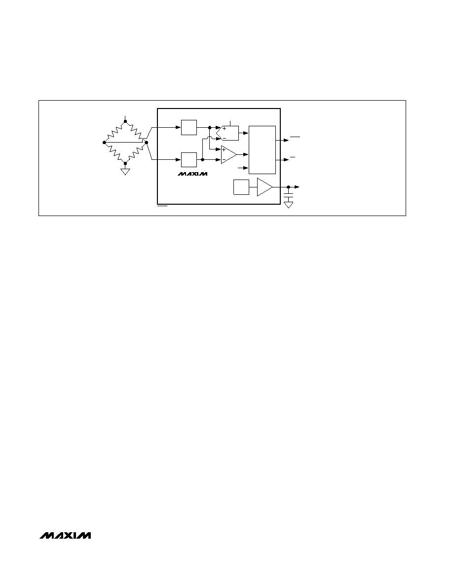
Strain-Gauge Operation
Connect the differential inputs of the MAX1407/
MAX1408/MAX1409/MAX1414 to the bridge network of
the strain gauge as shown in Figure 29. When connect-
ed to the internal reference, the ADC can resolve below
10V at the differential inputs. The internal buffers pro-
vide a high input impedance as long as the signal is
within the reduced common-mode range of the input
buffers. The bridge may also be driven directly from the
supply voltage. In this configuration, the ADC first mea-
sures the supply voltage and then the differential input
in sequence, and then calculates the ratio.
Grounding and Layout
For best performance, use printed circuit boards with
separate analog and digital ground planes. The device
perfomance will be highly degraded when using wire-
wrap boards.
Design the printed circuit board so that the analog and
digital sections are separated and confined to different
areas of the board. Join the digital and analog ground
planes at one point. If the MAX1407/MAX1408/
MAX1409/MAX1414 is the only device requiring an
AGND to DGND connection, then the ground planes
should be connected at the AGND pin of the MAX1407/
MAX1408/MAX1409/MAX1414. In systems where multi-
ple devices require AGND to DGND connections, the
connection should still be made at only one point. Make
the star ground as close to the MAX1407/MAX1408/
MAX1409/MAX1414 as possible.
Avoid running digital lines under the device because
these may couple noise onto the die. Run the analog
ground plane under the MAX1407/MAX1408/
MAX1409/MAX1414 to minimize coupling of digital
noise. Make the power-supply lines to the MAX1407/
MAX1408/MAX1409/MAX1414 as wide as possible to
provide low-impedance paths and reduce the effects of
glitches on the power-supply line.
Shield fast switching signals such as clocks with digital
ground to avoid radiating noise to other sections of the
board. Avoid running clock signals near the analog
inputs. Avoid crossover of digital and analog signals.
Traces on opposite sides of the board should run at
right angles to each other. This will reduce the effects
of feedthrough on the board. A microstrip technique is
best, but is not always possible with double-sided
boards. In this technique, the component side of the
board is dedicated to ground planes while signals are
placed on the solder side.
Good coupling is important when using high-resolution
ADCs. Decouple all analog supplies with 1F capaci-
tors in parallel with 0.1F HF ceramic capacitors to
AGND. Place these components as close to the device
as possible to achieve the best decoupling.
Crystal Layout
Since it is possible for noise to be coupled onto the
crystal pins, care must be taken when placing the
external crystal on a PC board layout. It is very impor-
tant to follow a few basic layout guidelines concerning
Figure 29. Strain-Gauge Application Circuit
MAX1407
MAX1408
MAX1414
REF
DRDY NOT AVAILABLE ON THE MAX1409
BAND
GAP
WAKE-UP
INTERRUPT
GENERATOR
REF
DRDY
INT
IN1
4.7
F
BUF
8:1
MUX
16-BIT ADC
CMP
REF OR AVDD
IN0
8:1
MUX
RA
RB
RD
RC
相关PDF资料 |
PDF描述 |
|---|---|
| V300A3V3M200BL3 | CONVERTER MOD DC/DC 3.3V 200W |
| VI-24K-MY-S | CONVERTER MOD DC/DC 40V 50W |
| V300A3V3M200BG | CONVERTER MOD DC/DC 3.3V 200W |
| VI-24J-MY-S | CONVERTER MOD DC/DC 36V 50W |
| VI-24H-MY-S | CONVERTER MOD DC/DC 52V 50W |
相关代理商/技术参数 |
参数描述 |
|---|---|
| MAX1409EAP | 制造商:Maxim Integrated Products 功能描述:LOW-POWER, 16-BIT MULTICHANNEL DAS WITH INTER - Bulk |
| MAX140C/D | 功能描述:模数转换器 - ADC RoHS:否 制造商:Texas Instruments 通道数量:2 结构:Sigma-Delta 转换速率:125 SPs to 8 KSPs 分辨率:24 bit 输入类型:Differential 信噪比:107 dB 接口类型:SPI 工作电源电压:1.7 V to 3.6 V, 2.7 V to 5.25 V 最大工作温度:+ 85 C 安装风格:SMD/SMT 封装 / 箱体:VQFN-32 |
| MAX140CMH | 制造商:Maxim Integrated Products 功能描述:44 PINS MQFP PKG - Bulk |
| MAX140CMH+ | 制造商:Maxim Integrated Products 功能描述:ADC SGL DUAL SLOPE 3 1/2DIGIT LED 44MQFP - Rail/Tube |
| MAX140CMH+D | 功能描述:模数转换器 - ADC 3 1/2 Dgt ADC w/Ref CPump LED Drivers RoHS:否 制造商:Texas Instruments 通道数量:2 结构:Sigma-Delta 转换速率:125 SPs to 8 KSPs 分辨率:24 bit 输入类型:Differential 信噪比:107 dB 接口类型:SPI 工作电源电压:1.7 V to 3.6 V, 2.7 V to 5.25 V 最大工作温度:+ 85 C 安装风格:SMD/SMT 封装 / 箱体:VQFN-32 |
发布紧急采购,3分钟左右您将得到回复。