参数资料
| 型号: | MAX1494CCJ+T |
| 厂商: | Maxim Integrated |
| 文件页数: | 14/34页 |
| 文件大小: | 0K |
| 描述: | IC ADC W/LCD DRIVER 32-TQFP |
| 产品培训模块: | Lead (SnPb) Finish for COTS Obsolescence Mitigation Program |
| 标准包装: | 2,000 |
| 显示器类型: | LCD |
| 配置: | 7 段 + 2 个信号器 |
| 接口: | 串行 |
| 数字或字符: | A/D,4.5 位数字 |
| 电流 - 电源: | 960µA |
| 电源电压: | 2.7 V ~ 5.25 V |
| 工作温度: | 0°C ~ 70°C |
| 安装类型: | 表面贴装 |
| 封装/外壳: | 32-LQFP |
| 供应商设备封装: | 32-LQFP(7x7) |
| 包装: | 带卷 (TR) |
第1页第2页第3页第4页第5页第6页第7页第8页第9页第10页第11页第12页第13页当前第14页第15页第16页第17页第18页第19页第20页第21页第22页第23页第24页第25页第26页第27页第28页第29页第30页第31页第32页第33页第34页
�� �
�
�3.5-� and� 4.5-Digit,� Single-Chip� ADCs�
�with� LCD� Drivers�
�Table� 2.� Decimal-Point� Control� Table� (MAX1494)�
�DP_EN�
�0�
�0�
�0�
�0�
�1�
�1�
�1�
�1�
�DPSET1�
�0�
�0�
�1�
�1�
�0�
�0�
�1�
�1�
�DPSET2�
�0�
�1�
�0�
�1�
�0�
�1�
�0�
�1�
�DISPLAY� OUTPUT�
�18888�
�18888�
�18888�
�18888�
�1� 8� 8� 8.8�
�1� 8� 8.8� 8�
�1� 8.8� 8� 8�
�1.8� 8� 8� 8�
�ZERO� INPUT� READING�
�0�
�0�
�0�
�0�
�0.0�
�0.00�
�0.000�
�0.0000�
�Table� 3.� Decimal-Point� Control� Table� (MAX1492)�
�DP_EN�
�X�
�X�
�X�
�X�
�DPSET1�
�0�
�0�
�1�
�1�
�DPSET2�
�0�
�1�
�0�
�1�
�DISPLAY� OUTPUT�
�1� 8� 8.8�
�1� 8.8� 8�
�1.8� 8� 8�
�1888�
�ZERO� INPUT� READING�
�0.0�
�0.00�
�0.000�
�000�
�X� =� Don’t� care.�
�Table� 4.� LCD� During� Overrange� and�
�Underrange� Conditions�
�The� MAX1492/MAX1494� overrange� and� underrange�
�display� is� shown� in� Table� 4.�
�Reference�
�CONDITION�
�OVERRANGE�
�UNDERRANGE�
�MAX1492�
�1–� –� –�
�-1–� –� –�
�MAX1494�
�1–� –� –� –�
�-1–� –� –� –�
�The� MAX1492/MAX1494� reference� sets� the� full-scale�
�range� of� the� ADC� transfer� function.� With� a� nominal�
�2.048V� reference,� the� ADC� full-scale� range� is� ±2V� with�
�the� RANGE� bit� equal� to� 0.� With� the� RANGE� bit� set� to� 1,�
�the� full-scale� range� is� ±200mV.� A� decreased� reference�
�voltage� decreases� full-scale� range� (see� the� Transfer�
�X�
�Y�
�Z�
�Functions� section).�
�The� MAX1492/MAX1494� accept� either� an� external� ref-�
�BP1�
�f�
�a�
�b�
�erence� or� an� internal� reference.� The� INTREF� bit� selects�
�the� reference� mode� (see� the� Control� Register�
�(Read/Write)� section).�
�BP2�
�e�
�g�
�c�
�For� internal-reference� operation,� set� INTREF� to� 1,� con-�
�nect� REF-� to� GND� and� bypass� REF+� to� GND� with� a�
�BP3�
�DP�
�d�
�DP�
�4.7μF� capacitor.� The� internal� reference� provides� a� nom-�
�inal� 2.048V� source� between� REF+� and� GND.� The� inter-�
�nal-reference� temperature� coefficient� is� typically�
�40ppm/°C.�
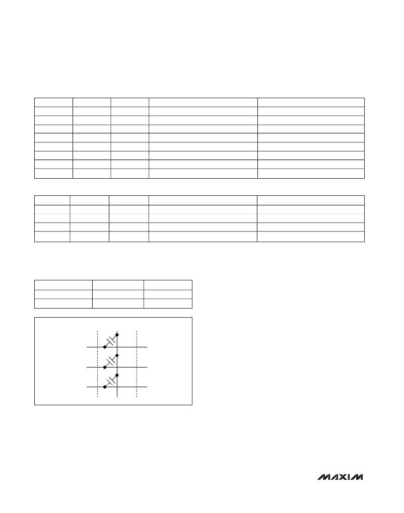
�Figure� 8.� Schematic� of� Display� Digit�
�The� MAX1492/MAX1494� allow� for� full� decimal-point� con-�
�trol� and� feature� leading� zero� suppression.� Use� the�
�DP_EN,� DPSET1,� and� DPSET2� bits� in� the� control� register�
�to� set� the� value� of� the� decimal� point.� Tables� 2� and� 3� show�
�the� truth� tables� of� the� DP_EN,� DPSET1,� and� DPSET2.� The�
�truth� tables� determine� decimal-point� usage.�
�The� default� power-on� state� sets� the� MAX1492/�
�MAX1494� to� use� the� external� reference� with� INTREF�
�cleared� to� 0.� The� external� reference� inputs,� REF+� and�
�REF-,� are� fully� differential.� For� a� valid� external-reference�
�input,� V� REF+� must� be� greater� than� V� REF-� .� Bypass� REF+�
�and� REF-� with� a� 0.1μF� or� greater� capacitor� to� GND� in�
�external-reference� mode.�
�14�
�______________________________________________________________________________________�
�相关PDF资料 |
PDF描述 |
|---|---|
| MAX15001BEUB+ | IC REG CTRLR PWM CM 10-UMAX |
| MAX15002ATL+T | IC REG CTRLR BUCK PWM 40-TQFNEP |
| MAX15003ATM+T | IC REG CTRLR BUCK PWM 48TQFN-EP |
| MAX15005AAUE/V+ | IC REG CTRLR PWM CM 16-TSSOP |
| MAX15006BASA+ | IC REG LDO 5V 50MA 8-SOIC |
相关代理商/技术参数 |
参数描述 |
|---|---|
| MAX1494EVC16 | 功能描述:模数转换器 - ADC MAX1494C16 EVAL KIT RoHS:否 制造商:Texas Instruments 通道数量:2 结构:Sigma-Delta 转换速率:125 SPs to 8 KSPs 分辨率:24 bit 输入类型:Differential 信噪比:107 dB 接口类型:SPI 工作电源电压:1.7 V to 3.6 V, 2.7 V to 5.25 V 最大工作温度:+ 85 C 安装风格:SMD/SMT 封装 / 箱体:VQFN-32 |
| MAX1494EVKIT | 功能描述:数据转换 IC 开发工具 Evaluation Kit/Evaluation System for the MAX1493 MAX1494 MAX1495 RoHS:否 制造商:Texas Instruments 产品:Demonstration Kits 类型:ADC 工具用于评估:ADS130E08 接口类型:SPI 工作电源电压:- 6 V to + 6 V |
| MAX14950ACTL+ | 功能描述:外围驱动器与原件 - PCI PCIe Gen III Re-Driver RoHS:否 制造商:PLX Technology 工作电源电压: 最大工作温度: 安装风格:SMD/SMT 封装 / 箱体:FCBGA-1156 封装:Tray |
| MAX14950ACTL+T | 功能描述:外围驱动器与原件 - PCI PCIe Gen III Re-Driver RoHS:否 制造商:PLX Technology 工作电源电压: 最大工作温度: 安装风格:SMD/SMT 封装 / 箱体:FCBGA-1156 封装:Tray |
| MAX14950CTO+ | 功能描述:外围驱动器与原件 - PCI PCIe Gen III Re-Driver RoHS:否 制造商:PLX Technology 工作电源电压: 最大工作温度: 安装风格:SMD/SMT 封装 / 箱体:FCBGA-1156 封装:Tray |
发布紧急采购,3分钟左右您将得到回复。