- 您现在的位置:买卖IC网 > PDF目录1838 > MAX16955AUE/V+ (Maxim Integrated Products)IC REG CTRLR BUCK PWM CM 16TSSOP PDF资料下载
参数资料
| 型号: | MAX16955AUE/V+ |
| 厂商: | Maxim Integrated Products |
| 文件页数: | 17/26页 |
| 文件大小: | 0K |
| 描述: | IC REG CTRLR BUCK PWM CM 16TSSOP |
| 其它有关文件: | Automotive Product Guide |
| 产品培训模块: | Lead (SnPb) Finish for COTS Obsolescence Mitigation Program |
| 标准包装: | 96 |
| PWM 型: | 电流模式 |
| 输出数: | 1 |
| 频率 - 最大: | 1MHz |
| 电源电压: | 3.5 V ~ 36 V |
| 降压: | 是 |
| 升压: | 无 |
| 回扫: | 无 |
| 反相: | 无 |
| 倍增器: | 无 |
| 除法器: | 无 |
| Cuk: | 无 |
| 隔离: | 无 |
| 工作温度: | -40°C ~ 125°C |
| 封装/外壳: | 16-TSSOP(0.173",4.40mm)裸露焊盘 |
| 包装: | 管件 |
�� �
�
�MAX16955�
�36V,� 1MHz� Step-Down� Controller�
�with� Low� Operating� Current�
�load� current.� The� switching� frequency� is� set� by� R� FOSC�
�(see� the� Setting� the� Switching� Frequency� section).�
�The� core� must� be� large� enough� not� to� saturate� at� the�
�peak� inductor� current� (I� PEAK� ):�
�The� MAX16955� uses� internal� frequency� independent�
�slope� compensation� to� ensure� stable� operation� at� duty�
�cycles� above� 50%.� The� maximum� slope� compensation�
�I� PEAK� =� I� LOAD� (� MAX� )� +�
�Δ� I� INDUCTOR�
�2�
�ramp� voltage� over� a� full� clock� period� is� 200mV.� Use� the�
�equation� below� to� select� the� inductor� value:�
�Transient� Response�
�The� inductor� ripple� current� also� impacts� transient�
�V� OUT� [� V� ]�
�L� [� μ� H� ]� ×� f� SW� [� MHz� ]�
�=� 1� ±� 25� %�
�response� performance,� especially� at� low� V� SUP� -� V� OUT�
�differentials.� Low� inductor� values� allow� the� inductor� cur-�
�rent� to� slew� faster,� replenishing� charge� removed� from�
�the� output� filter� capacitors� by� a� sudden� load� step.� The�
�However,� if� it� is� necessary,� higher� inductor� values� can�
�be� selected.�
�The� exact� inductor� value� is� not� critical� and� can� be�
�total� output� voltage� sag� is� the� sum� of� the� voltage� sag�
�while� the� inductor� is� ramping� up� and� the� voltage� sag�
�before� the� next� pulse� can� occur:�
�(� )�
�L� Δ� I� LOAD� (� MAX� )�
�adjusted to make trade-offs among size, cost, efficien-�
�cy,� and� transient� response� requirements.� Table� 1�
�shows� a� comparison� between� small� and� large� inductor�
�sizes.�
�V� SAG� =�
�2�
�2� C� OUT� (� (� V� SUP� � D� MAX� )� ?� V� OUT� )�
�+�
�Δ� I� LOAD(MAX )� (� t� ? Δ� t� )�
�C� OUT�
�Table� 1.� Inductor� Size� Comparison�
�INDUCTOR� SIZE�
�SMALLER� LARGER�
�Lower� price� Smaller� ripple�
�Smaller� form� factor� Higher� efficiency�
�where� D� MAX� is� the� maximum� duty� factor,� L� is� the� induc-�
�tor� value� in� μH,� C� OUT� is� the� output� capacitor� value� in�
�μF,� t� is� the� switching� period� (1/f� SW� )� in� μs,� and� Δ� t� equals�
�(V� OUT� /V� SUP� )� � t� when� in� fixed-frequency� PWM� mode,� or�
�L� � 0.2� � I� MAX� /(V� SUP� -� V� OUT� )� when� in� skip� mode.� The�
�amount� of� overshoot� (V� SOAR� )� during� a� full-load� to� no-�
�load� transient� due� to� stored� inductor� energy� can� be� cal-�
�(� Δ� I� LOAD� (� MAX� )� )�
�Larger� fixed-frequency� range�
�Faster� load� response�
�in� skip� mode�
�The� minimum� practical� inductor� value� is� one� that� caus-�
�es� the� circuit� to� operate� at� the� edge� of� critical� conduc-�
�culated� as:�
�V� SOAR�
�≈�
�2�
�2� C� OUT� V� OUT�
�L�
�tion� (where� the� inductor� current� just� touches� zero� with�
�every� cycle� at� maximum� load).� Inductor� values� lower�
�than� this� grant� no� further� size-reduction� benefit.� The�
�optimum� operating� point� is� usually� found� between� 25%�
�and� 45%� ripple� current.� When� pulse� skipping� (FSYNC�
�low� and� light� loads),� the� inductor� value� also� determines�
�the� load-current� value� at� which� PFM/PWM� switchover�
�occurs.�
�For� the� selected� inductance� value,� the� actual� peak-to-�
�peak� inductor� ripple� current� (� Δ� I� INDUCTOR� )� is� defined� by:�
�Current� Sensing�
�For� the� most� accurate� current� sensing,� use� a� current-�
�sense� resistor� (R� SENSE� )� between� the� inductor� and� the�
�output� capacitor.� Connect� CS� to� the� inductor� side� of�
�R� SENSE� ,� and� OUT� to� the� capacitor� side.� Dimension�
�R� SENSE� so� its� maximum� current� (I� OC� )� induces� a� voltage�
�of� V� LIMIT� (72mV� minimum)� across� R� SENSE� .�
�If� a� higher� voltage� drop� across� R� SENSE� must� be� tolerat-�
�ed,� divide� the� voltage� across� the� sense� resistor� with� a�
�voltage-divider� between� CS� and� OUT� to� reach� V� LIMIT�
�Δ� I� INDUCTOR� =�
�V� OUT� (� V� SUP� ?� V� OUT� )�
�V� SUP� � f� SW� � L�
�(72mV� minimum).�
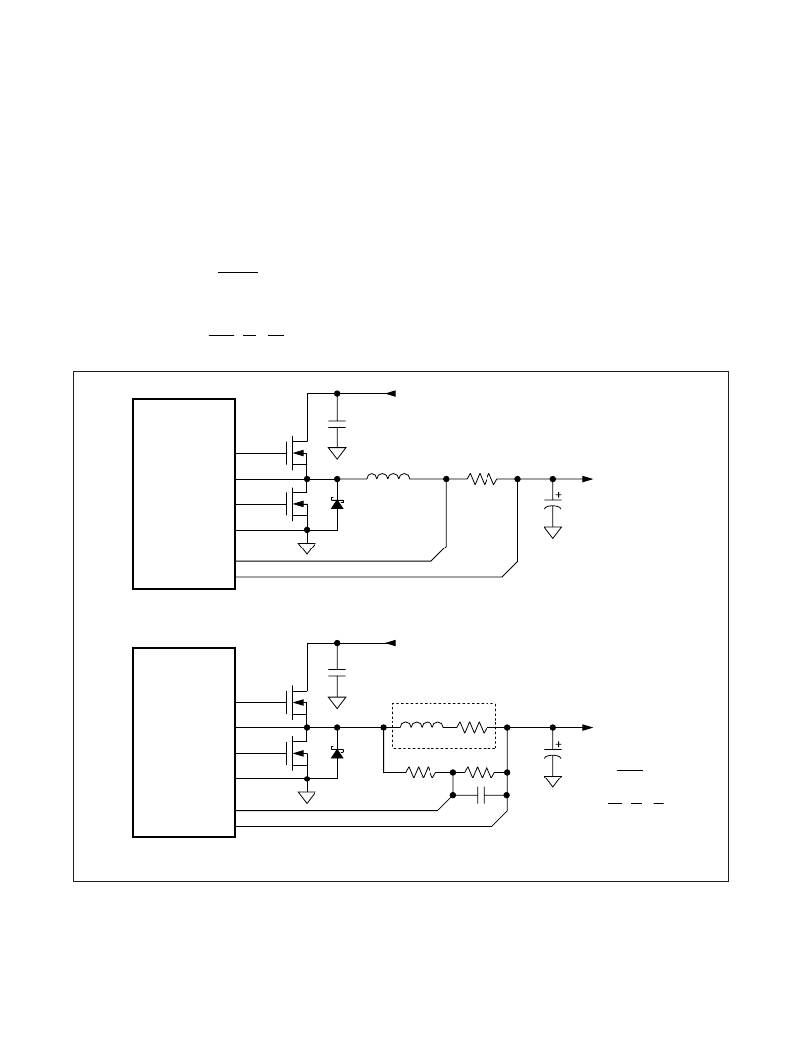
�The� current-sense� method� (Figure� 4)� and� magnitude�
�determine� the� achievable� current-limit� accuracy� and�
�where� Δ� I� INDUCTOR� is� in� mA,� L� is� in� μH,� and� f� SW� is� in� kHz.�
�Maxim� Integrated�
�power� loss.� Typically,� higher� current-sense� limits�
�provide� tighter� accuracy,� but� also� dissipate� more�
�power.� For� the� best� current-sense� accuracy� and� over-�
�current� protection,� use� a� ±1%� tolerance� current-sense�
�resistor� with� low� parasitic� inductance� between� the�
�inductor� and� output� as� shown� in� Figure� 4a.�
�17�
�相关PDF资料 |
PDF描述 |
|---|---|
| MAX16974AUE/V+ | IC REG BUCK SYNC 5V/ADJ 16TSSOP |
| MAX16975AEE/V+ | IC REG BUCK SYNC 5V/ADJ 16QSOP |
| MAX16976AEE/V+ | IC REG BUCK 5V/ADJ 0.6A 16QSOP |
| MAX16977SAUE/V+ | IC BUCK SYNC ADJ 2A 16TSSOP |
| MAX1697REUT#TG16 | IC REG SWITCHED CAP INV SOT23-6 |
相关代理商/技术参数 |
参数描述 |
|---|---|
| MAX16955EVKIT# | 功能描述:电源管理IC开发工具 MAX16955 Eval Kit RoHS:否 制造商:Maxim Integrated 产品:Evaluation Kits 类型:Battery Management 工具用于评估:MAX17710GB 输入电压: 输出电压:1.8 V |
| MAX16955EVKIT+ | 功能描述:电源管理IC开发工具 MAX16955 Eval Kit RoHS:否 制造商:Maxim Integrated 产品:Evaluation Kits 类型:Battery Management 工具用于评估:MAX17710GB 输入电压: 输出电压:1.8 V |
| MAX16956AUBA/V+T | 制造商:Maxim Integrated Products 功能描述:36V, 300MA, MINI BUCK CONVERTER WITH 2UA IQ - Tape and Reel |
| MAX16958GEE/V+ | 功能描述:模数转换器 - ADC 500mA Hi-Speed USB Protector RoHS:否 制造商:Texas Instruments 通道数量:2 结构:Sigma-Delta 转换速率:125 SPs to 8 KSPs 分辨率:24 bit 输入类型:Differential 信噪比:107 dB 接口类型:SPI 工作电源电压:1.7 V to 3.6 V, 2.7 V to 5.25 V 最大工作温度:+ 85 C 安装风格:SMD/SMT 封装 / 箱体:VQFN-32 |
| MAX16958GEE/V+T | 功能描述:模数转换器 - ADC 500mA Hi-Speed USB Protector RoHS:否 制造商:Texas Instruments 通道数量:2 结构:Sigma-Delta 转换速率:125 SPs to 8 KSPs 分辨率:24 bit 输入类型:Differential 信噪比:107 dB 接口类型:SPI 工作电源电压:1.7 V to 3.6 V, 2.7 V to 5.25 V 最大工作温度:+ 85 C 安装风格:SMD/SMT 封装 / 箱体:VQFN-32 |
发布紧急采购,3分钟左右您将得到回复。