- 您现在的位置:买卖IC网 > PDF目录1841 > MAX1889ETE+T (Maxim Integrated Products)IC PWR SUP TRPL LCD 16-TQFN PDF资料下载
参数资料
| 型号: | MAX1889ETE+T |
| 厂商: | Maxim Integrated Products |
| 文件页数: | 15/32页 |
| 文件大小: | 0K |
| 描述: | IC PWR SUP TRPL LCD 16-TQFN |
| 产品培训模块: | Lead (SnPb) Finish for COTS Obsolescence Mitigation Program |
| 标准包装: | 2,500 |
| 应用: | 控制器,TFT LCD |
| 输入电压: | 2.7 V ~ 5.5 V |
| 输出数: | 3 |
| 输出电压: | 2.7 V ~ 13 V |
| 工作温度: | 0°C ~ 85°C |
| 安装类型: | 表面贴装 |
| 封装/外壳: | 16-WQFN 裸露焊盘 |
| 供应商设备封装: | 16-TQFN-EP(5x5) |
| 包装: | 带卷 (TR) |
第1页第2页第3页第4页第5页第6页第7页第8页第9页第10页第11页第12页第13页第14页当前第15页第16页第17页第18页第19页第20页第21页第22页第23页第24页第25页第26页第27页第28页第29页第30页第31页第32页
�� �
�
�Triple-Output� TFT� LCD� Power� Supply�
�with� Fault� Protection�
�Positive� Linear-Regulator� Controller�
�The� positive� linear� regulator� provides� the� positive� high�
�voltage� for� the� TFT� LCD� gate� drivers.� The� high� voltage�
�can� be� produced� using� a� charge-pump� circuit� as� shown�
�in� Figure� 1.� Use� as� many� stages� as� necessary� to� obtain�
�the� required� output� voltage� (see� the� Selecting� the�
�Number� of� Charge-Pump� Stages� section).� The� positive�
�linear-regulator� controller� is� an� analog� gain� block� with� an�
�open-drain� N-channel� output.� It� drives� an� external� PNP�
�pass� transistor� with� a� 3k� ?� base-to-emitter� resistor� to�
�post-regulate� the� charge-pump� output� (Figure� 1).� The�
�regulator� controller� is� designed� to� be� stable� with� an� out-�
�put� capacitor� of� 0.1μF� or� more.�
�To� enable� the� regulator� using� an� external� control� signal,�
�apply� the� logic-control� input� in� series� with� a� signal�
�diode� (Figure� 1).� Additional� delay� can� be� added� with�
�external� circuitry.�
�Note� that� the� voltage� rating� of� the� DRVP� output� is� 28V.�
�If� higher� voltages� are� present,� an� external� cascode�
�NPN� transistor� should� be� used� with� the� emitter� con-�
�nected� to� DRVP,� the� base� to� V� MAIN� ,� and� the� collector� to�
�the� base� of� the� PNP.�
�Negative� Linear-Regulator� Controller�
�The� negative� linear� regulator� provides� the� negative� volt-�
�age� required� to� supply� gate� drivers� in� TFT� LCD� panels.�
�The� negative� voltage� can� be� produced� using� a� charge�
�pump� circuit� as� shown� in� Figure� 1.� Use� as� many� stages�
�as� necessary� to� obtain� the� required� output� voltage� (see�
�the� Selecting� the� Number� of� Charge-Pump� Stages� sec-�
�tion).� The� negative� linear-regulator� controller� is� an� ana-�
�log� gain� block� with� an� open-drain� P-channel� output.� It�
�drives� an� external� NPN� pass� transistor� with� a� 3k� ?� base-�
�to-emitter� resistor� to� postregulate� the� charge-pump� out-�
�IN�
�GATE�
�L�
�put� (Figure� 1).� The� regulator� controller� is� designed� to�
�be� stable� with� an� output� capacitor� of� 0.1μF� or� more.�
�The� negative� linear� regulator� is� enabled� as� soon� as� the�
�main� step-up� regulator� is� enabled.� To� enable� the� regula-�
�tor� using� an� external� control� signal,� apply� the� logic-control�
�input� through� an� open-drain� output� or� an� N-channel� MOS-�
�FET� (Figure� 1).� Additional� delay� can� be� added� with� exter-�
�nal� circuitry� (see� the� Applications� Information� section).�
�Note� that� the� voltage� rating� of� the� DRVN� output� is�
�V� IN� -� 28V.� If� higher� voltages� are� present,� an� external�
�cascode� PNP� transistor� should� be� used� with� the� emitter�
�connected� to� DRVN,� the� base� to� GND,� and� the� collec-�
�tor� to� the� base� of� the� NPN.�
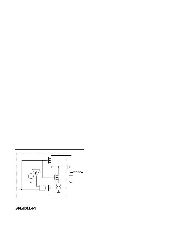
�Undervoltage� Lockout� (UVLO)�
�The� UVLO� comparator� of� the� MAX1889� compares� the�
�input� voltage� at� the� IN� pin� with� the� UVLO� threshold� (2.7V�
�rising,� 2.35V� falling,� typ)� to� ensure� that� the� input� voltage� is�
�high� enough� for� reliable� operation.� The� 350mV� (typ)� hys-�
�teresis� prevents� supply� transients� from� causing� a� restart.�
�Once� the� input� voltage� exceeds� the� UVLO� threshold,� the�
�controller� enables� the� reference� block.� Once� the� refer-�
�ence� is� above� 1.05V,� an� internal� 12μA� current� source�
�pulls� the� GATE� pin� low� and� turns� on� an� external� P-chan-�
�nel� MOSFET� switch� (P1,� Figure� 1)� that� connects� the� input�
�supply� to� the� regulator.� When� the� input� voltage� falls� below�
�the� UVLO� threshold,� the� controller� sets� the� fault� latch� and�
�pulls� GATE� high� with� an� internal� 100� ?� switch� to� turn� off�
�P1� quickly� (Figure� 4).�
�Reference� Voltage� (REF)�
�The� reference� output� is� nominally� 1.25V,� and� can�
�source� at� least� 50μA� (see� the� Typical� Operating�
�Characteristics� ).� Bypass� REF� with� a� 0.22μF� ceramic�
�capacitor� connected� between� REF� and� GND.�
�Oscillator� Frequency� (FREQ)�
�The� internal� oscillator� frequency� is� pin� programmable.�
�Connect� FREQ� to� ground� for� 500kHz� operation� and� to� V� IN�
�for� 1MHz� operation.� Note� that� the� soft-start� period� scales�
�with� the� oscillator� frequency� (see� the� Soft-Start� section).�
�Shutdown� (� SHDN� )�
�A� logic-low� signal� on� the� SHDN� pin� disables� all� device�
�0.625V�
�+�
�-�
�C� IN�
�functions� including� the� reference.� When� shut� down,� the�
�supply� current� drops� to� 0.1μA� (typ)� to� maximize� battery�
�life.� The� output� capacitance,� feedback� resistors,� and� load�
�current� determine� the� rate� at� which� each� output� voltage�
�EN�
�12� μ� A�
�decays.� A� logic-high� signal� on� the� SHDN� pin� activates� the�
�MAX1889� (see� the� Power-Up� Sequencing� section).� Do� not�
�leave� the� pin� floating.� If� unused,� connect� SHDN� to� IN.�
�Toggling� SHDN� or� cycling� IN� clears� the� fault� latch.�
�Figure� 4.� External� Input� P-Channel� MOSFET� Switch� Control�
�______________________________________________________________________________________�
�15�
�相关PDF资料 |
PDF描述 |
|---|---|
| MAX1896EUT#TG16 | IC REG BOOST ADJ 0.5A SOT23-6 |
| MAX1897ETP+T | IC REG CTRLR BUCK PWM 20-TQFN |
| MAX1898EUB42+T | IC CHARGER LI+ SNGL 10-UMAX |
| MAX1904ETJ+ | IC CNTRLR PWR SPLY LN 32-TQFN |
| MAX1917EEE+T | IC CNTRLR SYNC BUCK 16-QSOP |
相关代理商/技术参数 |
参数描述 |
|---|---|
| MAX1889EVKIT | 功能描述:电源管理IC开发工具 MAX1889 Eval Kit RoHS:否 制造商:Maxim Integrated 产品:Evaluation Kits 类型:Battery Management 工具用于评估:MAX17710GB 输入电压: 输出电压:1.8 V |
| MAX188ACAP | 功能描述:模数转换器 - ADC Integrated Circuits (ICs) RoHS:否 制造商:Texas Instruments 通道数量:2 结构:Sigma-Delta 转换速率:125 SPs to 8 KSPs 分辨率:24 bit 输入类型:Differential 信噪比:107 dB 接口类型:SPI 工作电源电压:1.7 V to 3.6 V, 2.7 V to 5.25 V 最大工作温度:+ 85 C 安装风格:SMD/SMT 封装 / 箱体:VQFN-32 |
| MAX188ACAP+ | 功能描述:模数转换器 - ADC 12-Bit 8Ch 133ksps 5.25V Precision ADC RoHS:否 制造商:Texas Instruments 通道数量:2 结构:Sigma-Delta 转换速率:125 SPs to 8 KSPs 分辨率:24 bit 输入类型:Differential 信噪比:107 dB 接口类型:SPI 工作电源电压:1.7 V to 3.6 V, 2.7 V to 5.25 V 最大工作温度:+ 85 C 安装风格:SMD/SMT 封装 / 箱体:VQFN-32 |
| MAX188ACAP+T | 功能描述:模数转换器 - ADC 12-Bit 8Ch 133ksps 5.25V Precision ADC RoHS:否 制造商:Texas Instruments 通道数量:2 结构:Sigma-Delta 转换速率:125 SPs to 8 KSPs 分辨率:24 bit 输入类型:Differential 信噪比:107 dB 接口类型:SPI 工作电源电压:1.7 V to 3.6 V, 2.7 V to 5.25 V 最大工作温度:+ 85 C 安装风格:SMD/SMT 封装 / 箱体:VQFN-32 |
| MAX188ACAP-T | 功能描述:模数转换器 - ADC RoHS:否 制造商:Texas Instruments 通道数量:2 结构:Sigma-Delta 转换速率:125 SPs to 8 KSPs 分辨率:24 bit 输入类型:Differential 信噪比:107 dB 接口类型:SPI 工作电源电压:1.7 V to 3.6 V, 2.7 V to 5.25 V 最大工作温度:+ 85 C 安装风格:SMD/SMT 封装 / 箱体:VQFN-32 |
发布紧急采购,3分钟左右您将得到回复。