- 您现在的位置:买卖IC网 > PDF目录1841 > MAX1997ETJ+T (Maxim Integrated Products)IC PWR SUPPLY TFT LCD 32TQFN PDF资料下载
参数资料
| 型号: | MAX1997ETJ+T |
| 厂商: | Maxim Integrated Products |
| 文件页数: | 11/31页 |
| 文件大小: | 0K |
| 描述: | IC PWR SUPPLY TFT LCD 32TQFN |
| 产品培训模块: | Lead (SnPb) Finish for COTS Obsolescence Mitigation Program |
| 标准包装: | 2,500 |
| 应用: | 控制器,TFT LCD |
| 输入电压: | 2.7 V ~ 5.5 V |
| 输出数: | 5 |
| 输出电压: | 2.7 V ~ 13 V |
| 工作温度: | 0°C ~ 85°C |
| 安装类型: | 表面贴装 |
| 封装/外壳: | 32-WFQFN 裸露焊盘 |
| 供应商设备封装: | 32-TQFN-EP(5x5) |
| 包装: | 带卷 (TR) |
第1页第2页第3页第4页第5页第6页第7页第8页第9页第10页当前第11页第12页第13页第14页第15页第16页第17页第18页第19页第20页第21页第22页第23页第24页第25页第26页第27页第28页第29页第30页第31页
�� �
�
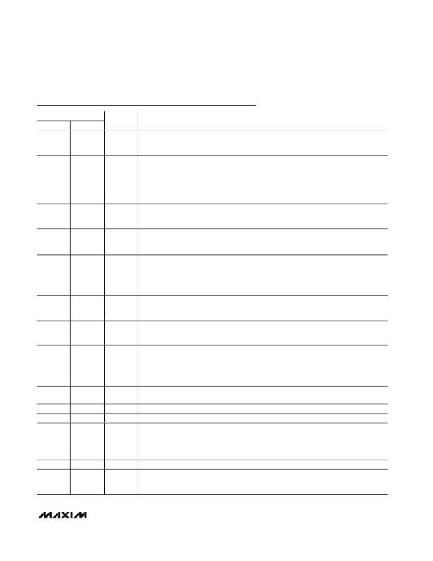
�Quintuple/Triple-Output� TFT� LCD� Power� Supplies�
�with� Fault� Protection� and� VCOM� Buffer�
�Pin� Description� (continued)�
�PIN�
�MAX1997� MAX1998�
�NAME�
�FUNCTION�
�Logic� Linear-Regulator� (REG� 1)� Feedback� Input.� FB1� regulates� at� 1.25V� nominal.� Connect�
�4�
�—�
�FB1�
�FB1� to� the� center� tap� of� a� resistive� voltage-divider� between� the� REG� 1� output� and� the� analog�
�ground� (GND)� to� set� the� output� voltage.� Place� the� resistive� voltage-divider� close� to� the� pin.�
�Sequence� Timing� Control� Input.� Connect� a� capacitor� from� this� pin� to� GND.� This� timing�
�capacitor� controls� the� turn-on� of� REG� P,� REG� N,� REG� 2,� and� DRVA.� The� sequence� timing�
�5�
�2�
�CT�
�block� is� enabled,� together� with� the� main� step-up� regulator,� when� ONDC� goes� high.� Then� an�
�internal� 5μA� current� source� charges� the� timing� capacitor� from� 0V� to� V� IN� ,� which� sets� the� turn-�
�on� delay.� A� discharge� switch� keeps� CT� at� GND� when� the� sequence� timing� block� is� disabled.�
�(See� the� Power-Up� Sequencing� and� Inrush� Current� Control� section.)�
�Gate-Off� Linear-Regulator� (REG� N)� Sequence� Control� Input.� REG� N� is� enabled� when� SHDN� is�
�6�
�3�
�ONN�
�high,� the� gate� to� the� input� P-channel� MOSFET� is� low,� ONDC� is� high,� and� V� CT� >� V� ON� N� .� (See�
�the� Power-Up� Sequencing� and� Inrush� Current� Control� section.)�
�Gate-On� Linear-Regulator� (REG� P)� Sequence� Control� Input.� REG� P� is� enabled� when� SHDN� is�
�7�
�4�
�ONP�
�high,� the� gate� to� the� input� P-channel� MOSFET� is� low,� ONDC� is� high,� and� V� CT� >� V� ONP� .� (See�
�the� Power-Up� Sequencing� and� Inrush� Current� Control� section.)�
�Gamma� Linear-Regulator� (REG� 2)� Sequence� Control� Input.� REG� 2� is� enabled� when� SHDN� is�
�high,� the� gate� to� the� input� P-channel� MOSFET� is� low,� ONDC� is� high,� and� V� CT� >� V� ON� 2� .� ON2�
�8�
�5�
�ON2�
�also� controls� the� DRVA� open-drain� output,� which� is� typically� used� to� turn� on� an� N-channel�
�MOSFET� between� the� step-up� regulator� output� and� the� source� driver� ICs� ’� supply� pins.� (See�
�the� Power-Up� Sequencing� and� Inrush� Current� Control� section.)�
�Gate-Off� Linear-Regulator� (REG� N)� Base� Drive.� Open� drain� of� an� internal� P-channel� MOSFET.�
�9�
�6�
�DRVN�
�Connect� DRVN� to� the� base� of� an� external� NPN� linear� regulator� pass� transistor.� (See� the� Pass�
�Transistor� Selection� section.)�
�Gate-Off� Linear-Regulator� (REG� N)� Feedback� Input.� FBN� regulates� to� 125mV� nominal.� Connect�
�10�
�7�
�FBN�
�FBN� to� the� center� tap� of� a� resistive� voltage-divider� between� the� REG� N� output� and� the� reference�
�voltage� (REF)� to� set� the� output� voltage.� Place� the� resistive� voltage-divider� close� to� the� pin.�
�Open-Drain� Sequence� Output.� The� DRVA� open-drain� output� is� controlled� by� ON2� .� DRVA� is�
�typically� used� to� turn� on� an� N-channel� MOSFET� between� the� step-up� regulator� output� and� the�
�11�
�8�
�DRVA�
�source-driver� ICs� ’� supply� pins.� DRVA� is� high� impedance� when� SHDN� is� high,� the� gate� to� the�
�input� P-channel� MOSFET� is� low,� ONDC� is� high,� and� V� CT� >� V� ON2� .� Otherwise,� DRVA� connects�
�to� ground.� (See� the� Power-Up� Sequencing� and� Inrush� Current� Control� section.)�
�12�
�13�
�14�
�15�
�16�
�17�
�9�
�10�
�—�
�—�
�—�
�—�
�REF�
�GND�
�FBNB�
�OUTB�
�V� DDB�
�FBPB�
�Internal� Reference� Bypass� Terminal.� Connect� a� 0.22μF� ceramic� capacitor� from� REF� to� the�
�analog� ground� (GND).� External� load� capability� is� at� least� 75μA.�
�Analog� Ground.�
�VCOM� Buffer� Inverting� Input.� (See� the� VCOM� Buffer� section.)�
�VCOM� Buffer� Output.� Requires� a� minimum� 0.47μF� ceramic� filter� capacitor� to� GND.� Place� the�
�capacitor� as� close� as� possible� to� OUTB.�
�VCOM� Buffer� Supply� Input.� Bypass� to� GND� with� a� 0.47μF� capacitor� as� close� as� possible� to�
�the� pin.�
�VCOM� Buffer� Noninverting� Input.� (See� the� VCOM� Buffer� section.)�
�Gamma� Linear-Regulator� (REG� 2)� Feedback� Input.� FBP� regulates� to� 1.25V� nominal.� Connect�
�18�
�—�
�FB2�
�FB2� to� the� center� tap� of� a� resistive� voltage-divider� between� the� REG� 2� output� and� the� analog�
�ground� (GND)� to� set� the� output� voltage.� Place� the� divider� close� to� the� pin.�
�______________________________________________________________________________________�
�11�
�相关PDF资料 |
PDF描述 |
|---|---|
| MAX256ASA+T | IC DRVR H-BRIDGE 8-SOIC |
| MAX3273ETG+T | IC LASR DRVR 2.7GBPS 3.6V 24TQFN |
| MAX3296CTI+T | IC LASR DRVR 2.5GBPS 5.5V 28TQFN |
| MAX3353EEUE+T | IC CHARGE PUMP USB OTG 16TSSOP |
| MAX3355EEUD+T | IC CHARGE PUMP USB OTG 14TSSOP |
相关代理商/技术参数 |
参数描述 |
|---|---|
| MAX1997EVKIT | 制造商:Maxim Integrated Products 功能描述:QUINTUPLE/TRIPLE OUTPUT TFT LCD POWER SUPPLIE - Bulk |
| MAX19983A | 功能描述:上下转换器 RoHS:否 制造商:Texas Instruments 产品:Down Converters 射频:52 MHz to 78 MHz 中频:300 MHz LO频率: 功率增益: P1dB: 工作电源电压:1.8 V, 3.3 V 工作电源电流:120 mA 最大功率耗散:1 W 最大工作温度:+ 85 C 安装风格:SMD/SMT 封装 / 箱体:PQFP-128 |
| MAX19985AETX+ | 功能描述:上下转换器 High-Gain 700MHz to 1GHz Downconv RoHS:否 制造商:Texas Instruments 产品:Down Converters 射频:52 MHz to 78 MHz 中频:300 MHz LO频率: 功率增益: P1dB: 工作电源电压:1.8 V, 3.3 V 工作电源电流:120 mA 最大功率耗散:1 W 最大工作温度:+ 85 C 安装风格:SMD/SMT 封装 / 箱体:PQFP-128 |
| MAX19985AETX+T | 功能描述:上下转换器 High-Gain 700MHz to 1GHz Downconv RoHS:否 制造商:Texas Instruments 产品:Down Converters 射频:52 MHz to 78 MHz 中频:300 MHz LO频率: 功率增益: P1dB: 工作电源电压:1.8 V, 3.3 V 工作电源电流:120 mA 最大功率耗散:1 W 最大工作温度:+ 85 C 安装风格:SMD/SMT 封装 / 箱体:PQFP-128 |
| MAX19985ETX+ | 功能描述:上下转换器 Dual, SiGe, .7-1GHz Downconversion Mixer RoHS:否 制造商:Texas Instruments 产品:Down Converters 射频:52 MHz to 78 MHz 中频:300 MHz LO频率: 功率增益: P1dB: 工作电源电压:1.8 V, 3.3 V 工作电源电流:120 mA 最大功率耗散:1 W 最大工作温度:+ 85 C 安装风格:SMD/SMT 封装 / 箱体:PQFP-128 |
发布紧急采购,3分钟左右您将得到回复。