- 您现在的位置:买卖IC网 > PDF目录1841 > MAX1997ETJ+T (Maxim Integrated Products)IC PWR SUPPLY TFT LCD 32TQFN PDF资料下载
参数资料
| 型号: | MAX1997ETJ+T |
| 厂商: | Maxim Integrated Products |
| 文件页数: | 19/31页 |
| 文件大小: | 0K |
| 描述: | IC PWR SUPPLY TFT LCD 32TQFN |
| 产品培训模块: | Lead (SnPb) Finish for COTS Obsolescence Mitigation Program |
| 标准包装: | 2,500 |
| 应用: | 控制器,TFT LCD |
| 输入电压: | 2.7 V ~ 5.5 V |
| 输出数: | 5 |
| 输出电压: | 2.7 V ~ 13 V |
| 工作温度: | 0°C ~ 85°C |
| 安装类型: | 表面贴装 |
| 封装/外壳: | 32-WFQFN 裸露焊盘 |
| 供应商设备封装: | 32-TQFN-EP(5x5) |
| 包装: | 带卷 (TR) |
第1页第2页第3页第4页第5页第6页第7页第8页第9页第10页第11页第12页第13页第14页第15页第16页第17页第18页当前第19页第20页第21页第22页第23页第24页第25页第26页第27页第28页第29页第30页第31页
�� �
�
�Quintuple/Triple-Output� TFT� LCD� Power� Supplies�
�with� Fault� Protection� and� VCOM� Buffer�
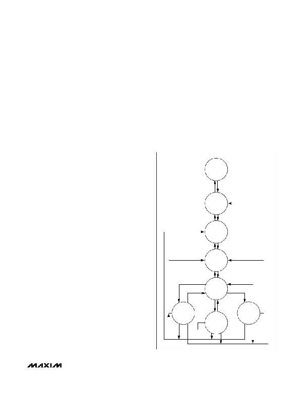
�Shutdown� (� SHDN� )�
�A� logic-low� signal� on� the� SHDN� pin� disables� all� device�
�functions� including� the� reference.� During� shutdown,� the�
�supply� current� drops� to� 0.1μA� (typ)� to� maximize� battery�
�life.� The� output� capacitance,� feedback� resistors,� and� load�
�current� determine� the� rate� at� which� each� output� voltage�
�decays.� A� logic-high� signal� on� the� SHDN� pin� activates� the�
�MAX1997/MAX1998.� (See� the� Power-Up� Sequencing�
�section.)� Do� not� leave� the� SHDN� pin� floating.� Toggling�
�SHDN� (below� 0.4V)� or� cycling� IN� (below� 2.2V)� clears� the�
�fault� latch.�
�Power-Up� Sequencing� and�
�Inrush� Current� Control�
�Once� SHDN� is� pulled� high� and� the� input� voltage� on� IN�
�exceeds� the� rising� input� UVLO� threshold� (2.7V� typ),� the�
�reference� turns� on.� With� a� 0.22μF� REF� bypass� capacitor,�
�the� reference� reaches� its� regulation� voltage� of� 1.25V� in�
�approximately� 1ms.� When� the� reference� voltage� is� ready,�
�the� MAX1997/MAX1998� enable� the� oscillator� and� fault�
�detector.� After� the� oscillator� is� enabled,� the� controller�
�(N1,� Figure� 1),� which� connects� the� main� step-up� regu-�
�lator� output� to� the� source� driver� ’� s� supply� pins.�
�Soft-Start�
�Each� positive� regulator� (MAIN,� REG� P,� REG� 1,� and� REG�
�2)� includes� a� 5-bit� soft-start� DAC� whose� input� is� the� ref-�
�erence,� and� whose� output� is� stepped� in� 32� steps� from�
�zero� up� to� the� reference� voltage.� The� soft-start� DAC� of� the�
�negative� regulator� (REG� N)� steps� from� the� reference�
�down� to� 125mV� in� 32� steps.� The� soft-start� duration� scales�
�with� the� switching� frequency� selected� and� is� 2.73ms� for�
�1.5MHz� operation,� 5.46ms� for� 750kHz� operation,� and�
�10.92ms� for� 375kHz� operation.�
�SHUTDOWN�
�turns� on� the� external� P-channel� MOSFET� P1� (Figure� 1)� by�
�pulling� GATE� low.� The� GATE� is� pulled� down� with� a� 10μA�
�current� source.� Add� a� capacitor� from� the� gate� of� P1� to� its�
�SHDN� =� 0� OR�
�V� IN� NOT�
�PRESENT�
�SHDN� =� 1� AND�
�V� IN� PRESENT�
�drain� to� slow� down� the� turn-on� rate� of� the� MOSFET,�
�which� reduces� inrush� current.�
�To� guarantee� slow� turn-on� at� lower� V� IN� ,� add� a� series�
�ENABLE� REF,�
�BIAS,� AND� UVLO�
�V� IN� <� 2.7V�
�resistor� between� the� GATE� pin� and� the� gate� of� the� exter-�
�V� IN� <� 2.7V�
�V� IN� >� 2.7V�
�nal� P-channel� MOSFET.� The� typical� value� of� the� resistor�
�ranges� between� 100k� ?� and� 200k� ?� .� Once� GATE� reaches�
�approximately� 0.6V,� an� internal� N-channel� MOSFET� turns�
�on� and� pulls� GATE� to� ground� in� order� to� maximize� the�
�GATE� NOT� READY�
�ENABLE� OSC,�
�OC� COMP,� GATE�
�CLEAR� FAULT�
�enhancement� of� the� external� P-channel� MOSFET.� After� P1�
�fully� turns� on,� REG� 1� and� the� fault� counter� are� enabled.�
�GATE� NOT� READY�
�GATE� READY�
�A� logic-high� signal� on� ONDC� enables� the� main� step-up�
�regulator� and� the� sequence� control� block.� The�
�sequence� control� state� diagram� is� shown� in� Figure� 7.�
�The� unique� sequence� control� block� allows� the� positive�
�ONDC� =� 0�
�ENABLE� REG� 1�
�AND� FAULT�
�COUNTER�
�ONDC� =� 0�
�ONDC� =� 1�
�ONDC� =� 0�
�gate-driver� voltage� (V� G_ON� ),� negative� gate-driver� volt-�
�age� (V� G_OFF� ),� and� the� source-driver� supply� voltage�
�(V� SOURCE� )� to� be� turned� on� in� any� order.� The� capacitor�
�at� the� CT� pin� is� kept� discharged� until� the� main� step-up�
�BOOST� SOFT-START�
�DONE� AND� V� CT� >� ONP�
�V� CT� <� ONP�
�ENABLE�
�BOOST,� VCOM,�
�SEQUENCE�
�BLOCK�
�V� CT� <� ON2�
�V� CT� >� ON2�
�regulator� is� enabled.� An� internal� 5μA� current� source�
�starts� charging� the� CT� capacitor� and� the� CT� voltage�
�ramps� linearly� up� to� approximately� V� IN� .� REG� P,� REG� N,�
�and� REG� 2� are� enabled� when� the� CT� voltage� exceeds�
�their� associated� ON_� control� inputs.� In� addition,� the�
�ENABLE� REG� P�
�V� CT� >� ONN� V� CT� <� ONN�
�ENABLE� REG� N�
�ENABLE� REG� 2,�
�DRVA� HIGH�
�IMPEDANCE�
�positive� linear� regulator� waits� for� the� completion� of� the�
�main� step-up� regulator� soft-start.� The� positive� linear�
�regulator� is� controlled� by� ONP� .� The� negative� linear� reg-�
�ulator� is� controlled� by� ONN� .� REG2� and� the� open-drain�
�output� DRVA� are� controlled� by� ON2� .� The� DRVA� signal�
�can� be� used� to� turn� on� an� external� N-channel� MOSFET�
�Figure� 7.� Power-Up� Sequence� State� Diagram�
�______________________________________________________________________________________�
�19�
�相关PDF资料 |
PDF描述 |
|---|---|
| MAX256ASA+T | IC DRVR H-BRIDGE 8-SOIC |
| MAX3273ETG+T | IC LASR DRVR 2.7GBPS 3.6V 24TQFN |
| MAX3296CTI+T | IC LASR DRVR 2.5GBPS 5.5V 28TQFN |
| MAX3353EEUE+T | IC CHARGE PUMP USB OTG 16TSSOP |
| MAX3355EEUD+T | IC CHARGE PUMP USB OTG 14TSSOP |
相关代理商/技术参数 |
参数描述 |
|---|---|
| MAX1997EVKIT | 制造商:Maxim Integrated Products 功能描述:QUINTUPLE/TRIPLE OUTPUT TFT LCD POWER SUPPLIE - Bulk |
| MAX19983A | 功能描述:上下转换器 RoHS:否 制造商:Texas Instruments 产品:Down Converters 射频:52 MHz to 78 MHz 中频:300 MHz LO频率: 功率增益: P1dB: 工作电源电压:1.8 V, 3.3 V 工作电源电流:120 mA 最大功率耗散:1 W 最大工作温度:+ 85 C 安装风格:SMD/SMT 封装 / 箱体:PQFP-128 |
| MAX19985AETX+ | 功能描述:上下转换器 High-Gain 700MHz to 1GHz Downconv RoHS:否 制造商:Texas Instruments 产品:Down Converters 射频:52 MHz to 78 MHz 中频:300 MHz LO频率: 功率增益: P1dB: 工作电源电压:1.8 V, 3.3 V 工作电源电流:120 mA 最大功率耗散:1 W 最大工作温度:+ 85 C 安装风格:SMD/SMT 封装 / 箱体:PQFP-128 |
| MAX19985AETX+T | 功能描述:上下转换器 High-Gain 700MHz to 1GHz Downconv RoHS:否 制造商:Texas Instruments 产品:Down Converters 射频:52 MHz to 78 MHz 中频:300 MHz LO频率: 功率增益: P1dB: 工作电源电压:1.8 V, 3.3 V 工作电源电流:120 mA 最大功率耗散:1 W 最大工作温度:+ 85 C 安装风格:SMD/SMT 封装 / 箱体:PQFP-128 |
| MAX19985ETX+ | 功能描述:上下转换器 Dual, SiGe, .7-1GHz Downconversion Mixer RoHS:否 制造商:Texas Instruments 产品:Down Converters 射频:52 MHz to 78 MHz 中频:300 MHz LO频率: 功率增益: P1dB: 工作电源电压:1.8 V, 3.3 V 工作电源电流:120 mA 最大功率耗散:1 W 最大工作温度:+ 85 C 安装风格:SMD/SMT 封装 / 箱体:PQFP-128 |
发布紧急采购,3分钟左右您将得到回复。