- 您现在的位置:买卖IC网 > PDF目录3764 > MAX3107EAG+T (Maxim Integrated Products)IC UART SPI/I2C 128 FIFO 24SSOP PDF资料下载
参数资料
| 型号: | MAX3107EAG+T |
| 厂商: | Maxim Integrated Products |
| 文件页数: | 40/52页 |
| 文件大小: | 0K |
| 描述: | IC UART SPI/I2C 128 FIFO 24SSOP |
| 产品培训模块: | Lead (SnPb) Finish for COTS Obsolescence Mitigation Program |
| 标准包装: | 1 |
| 特点: | 内部振荡器 |
| 通道数: | 4,QUART |
| FIFO's: | 128 字节 |
| 规程: | RS232,RS485 |
| 电源电压: | 2.35 V ~ 3.6 V |
| 带自动流量控制功能: | 是 |
| 带IrDA 编码器/解码器: | 是 |
| 带故障启动位检测功能: | 是 |
| 安装类型: | 表面贴装 |
| 封装/外壳: | 24-SSOP(0.209",5.30mm 宽) |
| 供应商设备封装: | 24-SSOP |
| 包装: | 标准包装 |
| 其它名称: | MAX3107EAG+TDKR |
第1页第2页第3页第4页第5页第6页第7页第8页第9页第10页第11页第12页第13页第14页第15页第16页第17页第18页第19页第20页第21页第22页第23页第24页第25页第26页第27页第28页第29页第30页第31页第32页第33页第34页第35页第36页第37页第38页第39页当前第40页第41页第42页第43页第44页第45页第46页第47页第48页第49页第50页第51页第52页
SPI/I2C UART with 128-Word FIFOs
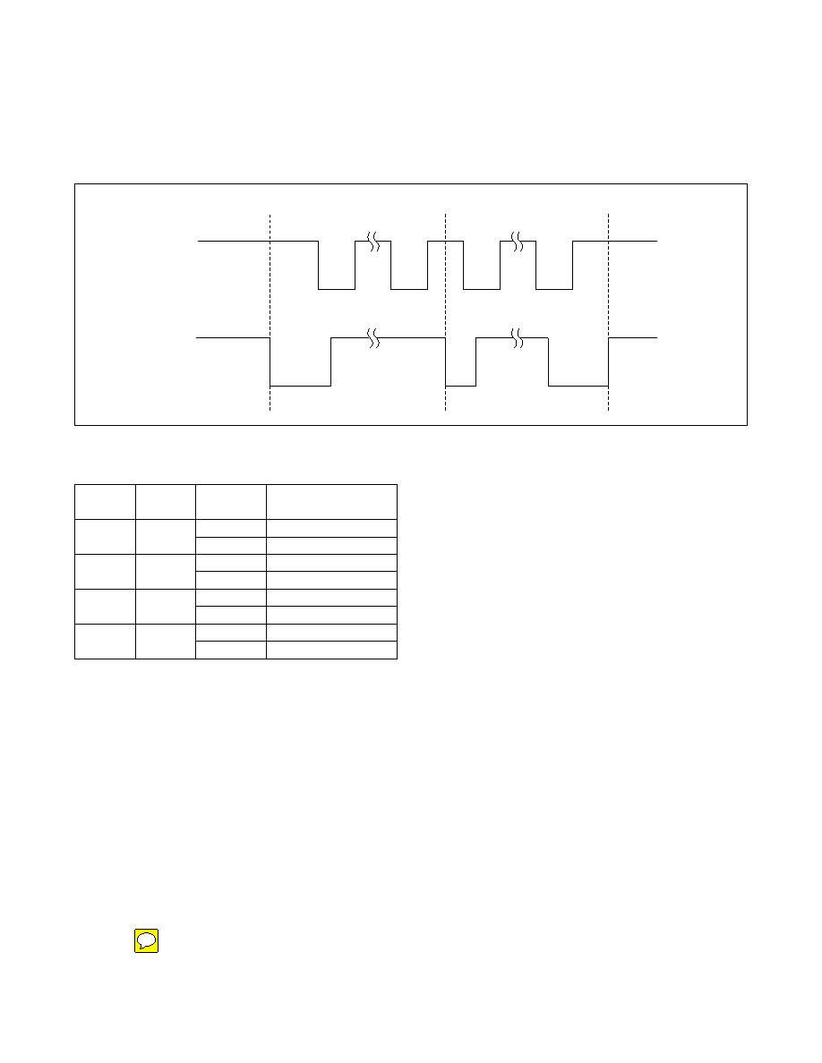
START, STOP, and Repeated START Conditions
When writing to the MAX3107 using I2C, the master
sends a START condition (S) followed by the MAX3107
I2C address. After the address, the master sends
the register address of the register that is to be pro-
grammed. The master then ends communication by
issuing a STOP condition (P) to relinquish control of the
bus, or a repeated START condition (Sr) to communicate
to another I2C slave. See Figure 17.
Slave Address
The MAX3107 includes a 7-bit slave address. The first 5
bits (MSBs) of the slave address are factory-programmed
and always 01011. These slave addresses are unique
device IDs. Connect A1, A0 to ground or VL to set the
I2C slave address (Table 5). The address is defined as
the 7 MSBs followed by the read/write bit. Set the read/
write bit to 1 to configure the MAX3107 to read mode. Set
the read/write bit to 0 to configure the MAX3107 to write
mode. The address is the first byte of information sent to
the MAX3107 after the START condition.
Bit Transfer
One data bit is transferred during each SCL clock cycle.
The data on SDA must remain stable during the high
period of the SCL clock pulse. Changes in SDA while
SCL is high and stable are considered control signals
(see the START, STOP, and Repeated START Conditions
section). Both SDA and SCL remain high when the bus
is not active.
Single-Byte Write
With this operation the master sends an address and 1
or 2 data bytes to the slave device (Figure 18). The write
byte procedure is as follows:
1) The master sends a START condition.
2) The master sends the 7-bit slave ID plus a write bit (low).
3) The addressed slave asserts an ACK on the data line.
4) The master sends the 8-bit register address.
5) The active slave asserts an ACK on the data line only
if the address is valid (NACK if not).
6) The master sends the 8-bit data byte.
7) The slave asserts an ACK on the data line.
8) The master generates a STOP condition.
Burst Write
With this operation the master sends an address and
multiple data bytes to the slave device (Figure 19). The
burst write procedure is as follows:
1) The master sends a START condition.
Figure 17. I2C START, STOP, and Repeated START Conditions
Table 5. I2C Address Map
SCL
SDA
S
Sr
P
DIN/A1
CS/A0
READ/
WRITE
I2C ADDRESS
0
W
0x58
R
0x59
0
1
W
0x5A
R
0x5B
1
0
W
0x5C
R
0x5D
1
W
0x5E
R
0x5F
Maxim Integrated
45
MAX3107
相关PDF资料 |
PDF描述 |
|---|---|
| SC28C94A1A,518 | IC UART QUAD W/FIFO 52-PLCC |
| SC16C754BIA68,518 | IC UART QUAD W/FIFO 68-PLCC |
| SC26C92C1N,602 | IC UART DUAL W/FIFO 40-DIP |
| SC28L91A1B,551 | IC UART SINGLE W/FIFO 44-PQFP |
| SC28L91A1B,528 | IC UART SINGLE W/FIFO 44PQFP |
相关代理商/技术参数 |
参数描述 |
|---|---|
| MAX3107ETG/V+ | 功能描述:UART 接口集成电路 UART RoHS:否 制造商:Texas Instruments 通道数量:2 数据速率:3 Mbps 电源电压-最大:3.6 V 电源电压-最小:2.7 V 电源电流:20 mA 最大工作温度:+ 85 C 最小工作温度:- 40 C 封装 / 箱体:LQFP-48 封装:Reel |
| MAX3107ETG/V+T | 功能描述:UART 接口集成电路 SPI/IC UART with 128-Word FIFOs and Internal Oscillator RoHS:否 制造商:Texas Instruments 通道数量:2 数据速率:3 Mbps 电源电压-最大:3.6 V 电源电压-最小:2.7 V 电源电流:20 mA 最大工作温度:+ 85 C 最小工作温度:- 40 C 封装 / 箱体:LQFP-48 封装:Reel |
| MAX3107ETG+ | 功能描述:UART 接口集成电路 SPI/I2C Compatible RoHS:否 制造商:Texas Instruments 通道数量:2 数据速率:3 Mbps 电源电压-最大:3.6 V 电源电压-最小:2.7 V 电源电流:20 mA 最大工作温度:+ 85 C 最小工作温度:- 40 C 封装 / 箱体:LQFP-48 封装:Reel |
| MAX3107ETG+T | 功能描述:UART 接口集成电路 SPI/I2C Compatible RoHS:否 制造商:Texas Instruments 通道数量:2 数据速率:3 Mbps 电源电压-最大:3.6 V 电源电压-最小:2.7 V 电源电流:20 mA 最大工作温度:+ 85 C 最小工作温度:- 40 C 封装 / 箱体:LQFP-48 封装:Reel |
| MAX3107EVKIT+ | 功能描述:UART 接口集成电路 UART with integrated Oscillator RoHS:否 制造商:Texas Instruments 通道数量:2 数据速率:3 Mbps 电源电压-最大:3.6 V 电源电压-最小:2.7 V 电源电流:20 mA 最大工作温度:+ 85 C 最小工作温度:- 40 C 封装 / 箱体:LQFP-48 封装:Reel |
发布紧急采购,3分钟左右您将得到回复。