- 您现在的位置:买卖IC网 > Datasheet目录43 > MAX5952CUAX+ (Maxim Integrated)IC PSE CNTRLR FOR POE 36-SSOP Datasheet资料下载
参数资料
| 型号: | MAX5952CUAX+ |
| 厂商: | Maxim Integrated |
| 文件页数: | 22/50页 |
| 文件大小: | 1006K |
| 描述: | IC PSE CNTRLR FOR POE 36-SSOP |
| 产品培训模块: | Lead (SnPb) Finish for COTS Obsolescence Mitigation Program |
| 标准包装: | 30 |
| 类型: | 以太网供电控制器(PoE) |
| 应用: | 远程外设(工业控制,相机,数据访问) |
| 内部开关: | 无 |
| 工作温度: | 0°C ~ 85°C |
| 安装类型: | 表面贴装 |
| 封装/外壳: | 36-BSOP(0.295",7.50mm 宽) |
| 供应商设备封装: | 36-SSOP |
| 包装: | 管件 |
第1页第2页第3页第4页第5页第6页第7页第8页第9页第10页第11页第12页第13页第14页第15页第16页第17页第18页第19页第20页第21页当前第22页第23页第24页第25页第26页第27页第28页第29页第30页第31页第32页第33页第34页第35页第36页第37页第38页第39页第40页第41页第42页第43页第44页第45页第46页第47页第48页第49页第50页
Watchdog
R1Dh, R1Eh, and R1Fh registers control the watchdog
operation. The watchdog function, when enabled, allows
the MAX5952 to gracefully take over control or securely
shuts down the power to the ports in case of software/
firmware crashes. Contact the factory for more details.
Address Inputs
A3, A2, A1, and A0 represent the four LSBs of the chip
address. The complete chip address is 7 bits (see
Table 4).
The four LSBs latch on the low-to-high transition of RESET
or after a power-supply start (either on V
DD
or V
EE
).
Address inputs default high through an internal 50k&
pullup resistor to V
DD
. The MAX5952 also responds to the
call through a global address 30h (see the Global
Addressing and Alert Response Protocol section).
I
2
C-Compatible Serial Interface
The MAX5952 operates as a slave that sends and
receives data through an I
2
C-compatible, 2-wire or
3-wire interface. The interface uses a serial-data input
line (SDAIN), a serial-data output line (SDAOUT), and a
serial-clock line (SCL) to achieve bidirectional commu-
nication between master(s) and slave(s). A master (typ-
ically a microcontroller) initiates all data transfers to and
from the MAX5952, and generates the SCL clock that
synchronizes the data transfer. In most applications,
connect the SDAIN and the SDAOUT lines together to
form the serial-data line (SDA).
Using the separate input and output data lines allows
optocoupling with the controller bus when an isolated
supply powers the microcontroller.
The MAX5952 SDAIN line operates as an input. The
MAX5952 SDAOUT operates as an open-drain output. A
pullup resistor, typically 4.7k&, is required on SDAOUT.
The MAX5952 SCL line operates only as an input. A
pullup resistor, typically 4.7k&, is required on SCL if
there are multiple masters, or if the master in a single-
master system has an open-drain SCL output.
High-Power, Quad, PSE Controller
for Power-Over-Ethernet
22 ______________________________________________________________________________________
0
1
0
A3
A2
A1
A0
R/W
Table 4. MAX5952 Address
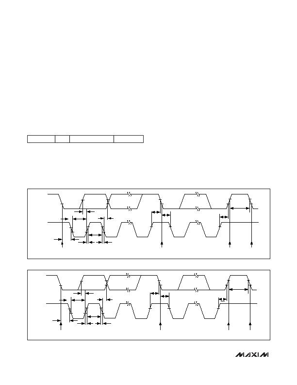
Figure 4. 2-Wire Serial Interface Timing Details
SCL
SDAIN
t
LOW
t
HIGH
t
R
t
F
t
BUF
START
CONDITION
STOP
CONDITION
REPEATED START CONDITION
START CONDITION
t
HD, STA
t
SU, DAT
t
HD, DAT
t
SU, STA
t
HD, STA
t
SU, STO
Figure 5. 3-Wire Serial Interface Timing Details
SCL
SDAIN/SDA
t
LOW
t
HIGH
t
R
t
F
t
BUF
START
CONDITION
STOP
CONDITION
REPEATED START CONDITION
START CONDITION
t
HD, STA
t
SU, DAT
t
HD, DAT
t
SU, STA
t
HD, STA
t
SU, STO
相关PDF资料 |
PDF描述 |
|---|---|
| MAX5953DUTM+ | IC INTERFACE 802.3AF 48TQFN |
| MAX5954LETX+T | IC PCI EXP/HOT-PLUG CTRLR 36TQFN |
| MAX5955BEEE+ | IC DUAL HOT-SWAP CTRLR 16-QSOP |
| MAX5957AETN+T | IC TRPL PCI EXP/HOT-PLUG 56-TQFN |
| MAX5960AECS+T | IC CTRLR HOT-PLUG QD 80-TQFP |
相关代理商/技术参数 |
参数描述 |
|---|---|
| MAX5952CUAX+ | 功能描述:热插拔功率分布 Quad PSE Controller for POE RoHS:否 制造商:Texas Instruments 产品:Controllers & Switches 电流限制: 电源电压-最大:7 V 电源电压-最小:- 0.3 V 工作温度范围: 功率耗散: 安装风格:SMD/SMT 封装 / 箱体:MSOP-8 封装:Tube |
| MAX5952CUAX+T | 功能描述:热插拔功率分布 Quad PSE Controller for POE RoHS:否 制造商:Texas Instruments 产品:Controllers & Switches 电流限制: 电源电压-最大:7 V 电源电压-最小:- 0.3 V 工作温度范围: 功率耗散: 安装风格:SMD/SMT 封装 / 箱体:MSOP-8 封装:Tube |
| MAX5952DEAX+ | 制造商:Maxim Integrated Products 功能描述:- Rail/Tube |
| MAX5952DEAX+T | 制造商:Maxim Integrated Products 功能描述:HIGH-POWER QUAD PSE CONTROLLER FOR - Tape and Reel |
| MAX5952DUAX+ | 制造商:Maxim Integrated Products 功能描述:- Rail/Tube |
发布紧急采购,3分钟左右您将得到回复。