- 您现在的位置:买卖IC网 > PDF目录13568 > MAX8952EWE+T (Maxim Integrated Products)IC REG BUCK SYNC ADJ 2.5A 16WLP PDF资料下载
参数资料
| 型号: | MAX8952EWE+T |
| 厂商: | Maxim Integrated Products |
| 文件页数: | 17/31页 |
| 文件大小: | 0K |
| 描述: | IC REG BUCK SYNC ADJ 2.5A 16WLP |
| 产品培训模块: | Lead (SnPb) Finish for COTS Obsolescence Mitigation Program |
| 标准包装: | 2,500 |
| 类型: | 降压(降压) |
| 输出类型: | 可调式 |
| 输出数: | 1 |
| 输出电压: | 0.77 V ~ 1.4 V |
| 输入电压: | 2.5 V ~ 5.5 V |
| 频率 - 开关: | 3.25MHz |
| 电流 - 输出: | 2.5A |
| 同步整流器: | 是 |
| 工作温度: | -40°C ~ 85°C |
| 安装类型: | 表面贴装 |
| 封装/外壳: | 16-UFBGA,WLCSP |
| 包装: | 带卷 (TR) |
| 供应商设备封装: | 16-WLP(2x2) |
第1页第2页第3页第4页第5页第6页第7页第8页第9页第10页第11页第12页第13页第14页第15页第16页当前第17页第18页第19页第20页第21页第22页第23页第24页第25页第26页第27页第28页第29页第30页第31页
�� �
�
�MAX8952�
�2.5A� Step-Down� Regulator�
�with� Remote� Sense� in� 2mm� x� 2mm� WLP�
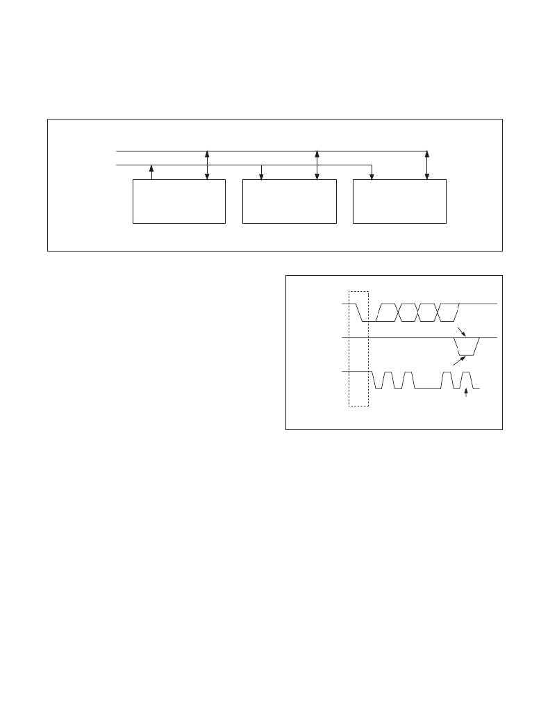
�SDA�
�SCL�
�MASTER�
�TRANSMITTER/RECEIVER�
�Figure� 11.� I� 2� C� Master/Slave� Configuration�
�a� STOP� condition� (see� the� Acknowledge� section� for�
�more� information).� The� STOP� condition� frees� the� bus.�
�To� issue� a� series� of� commands� to� the� slave,� the� master�
�SLAVE� RECEIVER�
�SDA� OUTPUT�
�SLAVE�
�TRANSMITTER/RECEIVER�
�can� issue� REPEATED� START� (Sr)� commands� instead� of�
�a� STOP� command� to� maintain� control� of� the� bus.� In�
�FROM� TRANSMITTER�
�D7�
�D6�
�D0�
�general,� a� REPEATED� START� command� is� functionally�
�equivalent� to� a� regular� START� command.�
�When� a� STOP� condition� or� incorrect� address� is� detect-�
�SDA� OUTPUT�
�FROM� RECEIVER�
�NOT� ACKNOWLEDGE�
�ed,� the� IC� internally� disconnects� SCL� from� the� serial�
�interface� until� the� next� START� condition,� minimizing� dig-�
�ital� noise� and� feedthrough.�
�SCL� FROM�
�MASTER�
�1�
�2�
�ACKNOWLEDGE�
�8�
�9�
�System� Configuration�
�A� device� on� the� I� 2� C� bus� that� generates� a� message� is�
�called� a� transmitter� and� a� device� that� receives� the� mes-�
�sage� is� a� receiver.� The� device� that� controls� the� mes-�
�sage� is� the� master� and� the� devices� that� are� controlled�
�by� the� master� are� called� slaves.� See� Figure� 11.�
�START� CONDITION�
�Figure� 12.� I� 2� C� Acknowledge�
�CLOCK� PULSE� FOR�
�ACKNOWLEDGEMENT�
�Acknowledge�
�The� number� of� data� bytes� between� the� START� and�
�STOP� conditions� for� the� transmitter� and� receiver� are�
�unlimited.� Each� 8-bit� byte� is� followed� by� an� acknowl-�
�edge� bit.� The� acknowledge� bit� is� a� low-level� signal� put�
�on� SDA� by� the� receiver� during� which� time� the� master�
�generates� an� extra� acknowledge-related� clock� pulse.� A�
�slave� receiver� that� is� addressed� must� generate� an�
�acknowledge� after� each� byte� it� receives.� Also,� a� master�
�receiver� must� generate� an� acknowledge� after� each�
�byte� it� receives� that� has� been� clocked� out� of� the� slave�
�transmitter.� See� Figure� 12.�
�The� device� that� acknowledges� must� pull� down� the� SDA�
�line� during� the� acknowledge� clock� pulse,� so� that� the�
�SDA� line� is� stable� low� during� the� high� period� of� the�
�Maxim� Integrated�
�acknowledge� clock� pulse� (setup� and� hold� times� must�
�also� be� met).� A� master� receiver� must� signal� an� end� of�
�data� to� the� transmitter� by� not� generating� an� acknowl-�
�edge� on� the� last� byte� that� has� been� clocked� out� of� the�
�slave.� In� this� case,� the� transmitter� must� leave� SDA� high�
�to� enable� the� master� to� generate� a� STOP� condition.�
�Register� Reset�
�The� I� 2� C� resisters� reset� back� to� their� default� values� when�
�the� voltage� at� either� IN1� or� V� DD� drops� below� the�
�corresponding� UVLO� threshold� (see� the� Electrical�
�Characteristics� table).�
�Update� of� Output� Operation� Mode�
�If� updating� the� output� voltage� or� Operation� Mode� regis-�
�ter� for� the� mode� that� the� IC� is� currently� operating� in,� the�
�17�
�相关PDF资料 |
PDF描述 |
|---|---|
| SC1608C-331 | INDUCTOR SMD 330UH 0.07A 100KHZ |
| SC1608C-330 | INDUCTOR SMD 33UH 0.27A 100KHZ |
| VI-JNK-EX-F2 | CONVERTER MOD DC/DC 40V 75W |
| SC1608C-2R2 | INDUCTOR SMD 2.2UH 0.92A 1.0MHZ |
| VI-JNK-EX-F1 | CONVERTER MOD DC/DC 40V 75W |
相关代理商/技术参数 |
参数描述 |
|---|---|
| MAX8954EWN+ | 制造商:Maxim Integrated Products 功能描述:PMIC FOR PICO PROJECTORS - Rail/Tube |
| MAX8954EWN+T | 制造商:Maxim Integrated Products 功能描述:PMIC FOR PICO PROJECTORS - Tape and Reel |
| MAX8958EWW+ | 制造商:Maxim Integrated Products 功能描述:COMPLETE PMIC FOR INTEL ATOM PROCESSOR-BASED PLATFORM - Rail/Tube |
| MAX8958EWW+T | 制造商:Maxim Integrated Products 功能描述:COMPLETE PMIC FOR INTEL ATOM PROCESSOR-BASED PLATFORM - Tape and Reel 制造商:Maxim Integrated Products 功能描述:COMPLETE POWER MANAGEMENT IC FOR INTEL'S |
| MAX8959EVKIT+ | 制造商:Maxim Integrated Products 功能描述:PMIC FOR BROADCOM 2.5G SMART PHONE - Boxed Product (Development Kits) |
发布紧急采购,3分钟左右您将得到回复。