- 您现在的位置:买卖IC网 > PDF目录80516 > MB91F465PAPMC-GSE2 (FUJITSU LTD) RISC MICROCONTROLLER, PQFP176 PDF资料下载
参数资料
| 型号: | MB91F465PAPMC-GSE2 |
| 厂商: | FUJITSU LTD |
| 元件分类: | 微控制器/微处理器 |
| 英文描述: | RISC MICROCONTROLLER, PQFP176 |
| 封装: | 24 X 24 MM, 0.50 MM PITCH, LEAD FREE, PLASTIC, LQFP-176 |
| 文件页数: | 198/200页 |
| 文件大小: | 6566K |
| 代理商: | MB91F465PAPMC-GSE2 |
第1页第2页第3页第4页第5页第6页第7页第8页第9页第10页第11页第12页第13页第14页第15页第16页第17页第18页第19页第20页第21页第22页第23页第24页第25页第26页第27页第28页第29页第30页第31页第32页第33页第34页第35页第36页第37页第38页第39页第40页第41页第42页第43页第44页第45页第46页第47页第48页第49页第50页第51页第52页第53页第54页第55页第56页第57页第58页第59页第60页第61页第62页第63页第64页第65页第66页第67页第68页第69页第70页第71页第72页第73页第74页第75页第76页第77页第78页第79页第80页第81页第82页第83页第84页第85页第86页第87页第88页第89页第90页第91页第92页第93页第94页第95页第96页第97页第98页第99页第100页第101页第102页第103页第104页第105页第106页第107页第108页第109页第110页第111页第112页第113页第114页第115页第116页第117页第118页第119页第120页第121页第122页第123页第124页第125页第126页第127页第128页第129页第130页第131页第132页第133页第134页第135页第136页第137页第138页第139页第140页第141页第142页第143页第144页第145页第146页第147页第148页第149页第150页第151页第152页第153页第154页第155页第156页第157页第158页第159页第160页第161页第162页第163页第164页第165页第166页第167页第168页第169页第170页第171页第172页第173页第174页第175页第176页第177页第178页第179页第180页第181页第182页第183页第184页第185页第186页第187页第188页第189页第190页第191页第192页第193页第194页第195页第196页第197页当前第198页第199页第200页
MB91460P Series
DS07-16615-2E
97
7.
Data Flash parallel programming mode
Note: The currently available parallel flash programmers do not support the programming of the data flash. The
programmers may be updated on request. This chapter is for information only.
7.1.
Flash configuration in parallel Flash programming mode
Parallel Flash programming mode (MD[2:0] = 111):
MB91F467PA
Note: The address in parallel programming mode is listed here without 10:0000h offset.
Set the offset by keeping FA[22:20] = 001 the same kind as used for programming of the main flash
.
Note: The “Dummy addresses for auto algorithm” are accepted although they are located below the physical
addresses of the flash macro. This address space is needed to apply correct addresses in auto algorithms.
See the example in ”Auto Program Algorithms’ on page 86 .
7.2.
Address mapping from CPU to parallel programming mode
The following tables show the calculation from CPU addresses to data flash macro addresses which are used
in parallel programming.
7.2.1.
Address mapping MB91F467PA
Note: FA result is without 10:0000h offset for parallel Flash programming .
Set the offset by keeping FA[22:20] = 001 the same kind as used for programming of the main flash
.
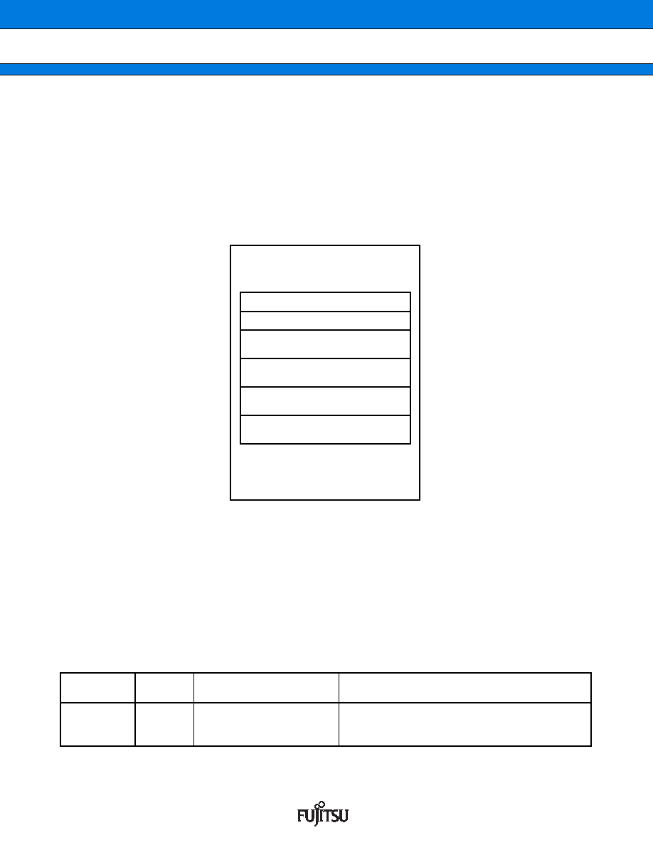
CPU Address
(addr)
Condition
Flash
sectors
FA (flash address) Calculation
FFFB:FF00h
to
FFFC:FFFFh
-
SAS, SA0, SA1, SA2, SA3
(256 Byte + 64 Kbyte)
FA := addr - 0B:0000h
FFFC 0000H
FFFD 0000H
External bus area
FFFF FFFFH
0050 0000H
FFFB FF00H
FFFC C000H
FFFC 4000H
FFFC 8000H
External bus area
Data Flash Security Sector (256 Byte)
Data Flash Sector 3 (16 KB)
Data Flash Sector 2 (16 KB)
Data Flash Sector 1 (16 KB)
Data Flash Sector 0 (16 KB)
01 0000H
01 FFFFH
00 FF00H
01 C000H
01 4000H
01 8000H
CPU
address
Parallel
programming
mode
address
FFFB F000H
Dummy addresses for auto algorithm
相关PDF资料 |
PDF描述 |
|---|---|
| MB95F353LPF-G-SNE2 | MICROCONTROLLER, PDSO24 |
| MPC8560CVT667JC | 32-BIT, 667 MHz, RISC PROCESSOR, PBGA783 |
| M926-02I622.0800 | 622.08 MHz, OTHER CLOCK GENERATOR, CQCC36 |
| M928-02-700.0000 | 700 MHz, OTHER CLOCK GENERATOR, CQCC36 |
| MK1411SLF | 35.46896 MHz, VIDEO CLOCK GENERATOR, PDSO8 |
相关代理商/技术参数 |
参数描述 |
|---|---|
| MB91F465X | 制造商:FUJITSU 制造商全称:Fujitsu Component Limited. 功能描述:The Ultimate Automotive Network |
| MB91F465XAPMC-ESE2 | 制造商:FUJITSU 功能描述: |
| MB91F465XAPMC-GE1 | 制造商:FUJITSU 功能描述: |
| MB91F466BA | 制造商:FUJITSU 制造商全称:Fujitsu Component Limited. 功能描述:32-bit Microcontroller |
| MB91F466HAPMC-GSE2 | 制造商:FUJITSU 功能描述: |
发布紧急采购,3分钟左右您将得到回复。